
A high-current silicon-on-insulator lateral insulated gate bipolar transistor device

A bipolar transistor and silicon-on-insulator technology, applied in the field of power semiconductor devices, can solve the problems of small current capacity and small chip area, and achieve the effects of increasing current capacity, small on-state voltage drop, and increasing carrier density

Active Publication Date: 2019-03-12
SOUTHEAST UNIV
View PDF3 Cites 0 Cited by
  • Summary
  • Abstract
  • Description
  • Claims
  • Application Information

AI Technical Summary

Problems solved by technology

However, the small current capability of SOI-LIGBT devices is the bottleneck that restricts the power module to work at a higher frequency, with better energy efficiency and smaller chip area.

Method used


Image

  • A high-current silicon-on-insulator lateral insulated gate bipolar transistor device
  • A high-current silicon-on-insulator lateral insulated gate bipolar transistor device
  • A high-current silicon-on-insulator lateral insulated gate bipolar transistor device

Examples


Embodiment Construction

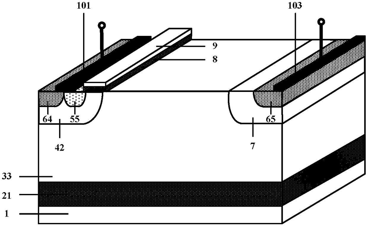
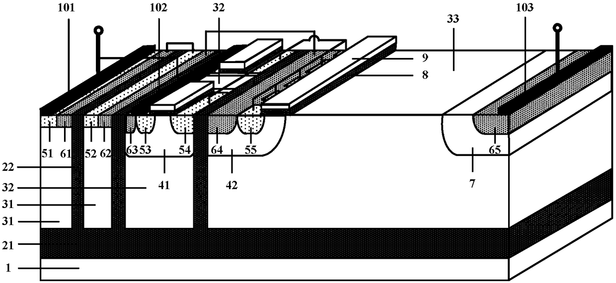
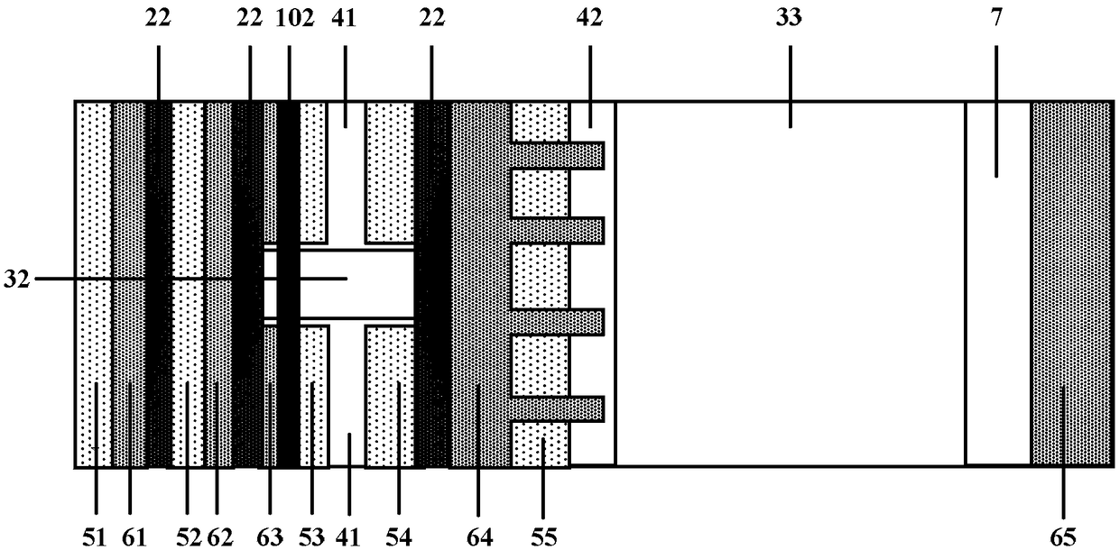
[0028] Combine below Figure 2-3 , to describe the present invention in detail, a large current silicon-on-insulator lateral insulated gate bipolar transistor device, comprising: a P-type substrate 1, a buried oxygen 21 is arranged on the P-type substrate 1, and a buried oxygen 21 is arranged above the buried oxygen 21 There is an N-type epitaxial layer 3, which is characterized in that an isolation oxide layer 22 is provided in the N-type epitaxial layer 3, and the isolation oxide layer 22 separates the N-type epitaxial layer 3 into a first N-type epitaxial layer 31, a second N-type epitaxial layer 31, and a second N-type epitaxial layer 31. -type epitaxial layer 32 and the third N-type epitaxial layer 33, the second P-type body region 42 and the N-type buffer layer 7 are provided on the third N-type epitaxial layer 33 top, and the second P-type body region 42 is provided on the top It is provided that the N-type emitter 55 is connected with the second heavily doped P region ...


PUM


Abstract

The invention relates to a high-current silicon-on-insulator transverse insulated gate bipolar transistor device. The device comprises a P-type substrate; a buried oxide is arranged on the P-type substrate; an N-type epitaxial layer is arranged on the buried oxide, wherein the N-type epitaxial layer is divided into a first N-type epitaxial layer, a second N-type epitaxial layer and a third N-type epitaxial layer trough isolation oxide layers; a second P-type body region and an N type buffer layer are arranged at the upper part of the third N-type epitaxial layer; an N-type emitter and an interdigitated second heavily doped P region are arranged in the second P-type body region; a gate oxide layer and a polysilicon gate are arranged on the second P-type body region; a P-type collector is arranged in the N type buffer layer and is adopted as the anode of the device; an anode metal layer is arranged on the P-type collector; at least two first P-type body regions are arranged at the upper part of the second N-type epitaxial layer; N-type MOS transistors are arranged in the at least two first P-type body regions respectively; at least two series diodes are arranged at the upper part of the first N-type epitaxial layer; isolation oxide layers are arranged between adjacent diodes; the N-type emitter is connected with all N-type drains; the second heavily doped P region is connected with the anodes of the series diodes; N-type sources and first heavily doped P regions are connected with the cathode of the tail end diode of the series diodes; and the cathode of the tail end diode of the series diodes is adopted as the cathode of the device.

Description

technical field [0001] The invention mainly relates to the technical field of power semiconductor devices, in particular to a large-current silicon-on-insulator lateral insulated gate bipolar transistor device, which is especially suitable for single-chip integrated power chips and intelligent power modules. Background technique [0002] Insulated Gate Bipolar Transistor (IGBT) is a composite power device evolved from the combination of MOS gate device structure and bipolar transistor structure. It has the characteristics of both MOS transistor and bipolar transistor, and has good on-state current and The trade-off relationship between switching losses. Silicon-on-insulator lateral insulated gate bipolar transistor (SOI-Lateral InsulatedGate Bipolar Transistor, SOI-LIGBT) is a typical device based on SOI technology, which has the advantages of easy integration, high withstand voltage, strong drive current capability, and fast switching speed. It has been widely used in powe...

Claims


Application Information

Patent Timeline
Patent Type & Authority Patents(China)
IPC IPC(8): H01L29/739H01L29/06
CPCH01L29/0603H01L29/0615H01L29/0626H01L29/7393H01L29/7436
Inventor 祝靖卞方娟杨卓吴汪然宋慧滨孙伟锋陆生礼时龙兴
Owner SOUTHEAST UNIV
Learn More