Semiconductor structure and manufacturing method thereof

A manufacturing method and semiconductor technology, applied in semiconductor/solid-state device manufacturing, semiconductor devices, transistors, etc., can solve the problems of SRAM device electrical performance to be improved, and achieve the effect of avoiding adverse effects, reducing the degree of diffusion, and optimizing electrical performance

Active Publication Date: 2019-12-31
SEMICON MFG INT (SHANGHAI) CORP +1
View PDF4 Cites 0 Cited by
  • Summary
  • Abstract
  • Description
  • Claims
  • Application Information

AI Technical Summary

Problems solved by technology

[0005] However, the electrical performance of SRAM devices formed by the prior art still needs to be improved.

Method used


Image

  • Semiconductor structure and manufacturing method thereof
  • Semiconductor structure and manufacturing method thereof
  • Semiconductor structure and manufacturing method thereof

Examples


Embodiment Construction

[0036] It can be seen from the background art that the electrical performance of the SRAM device formed in the prior art needs to be improved. Combined with the manufacturing method of SRAM devices, the reasons are analyzed:

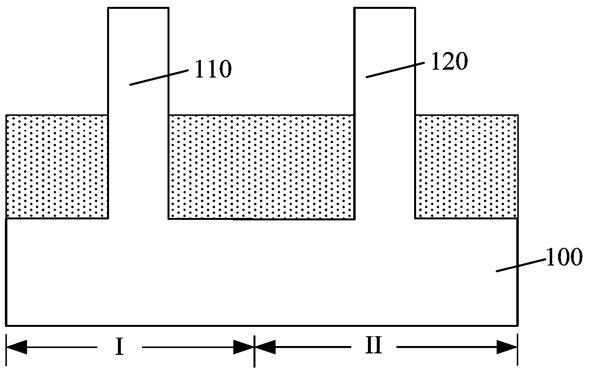
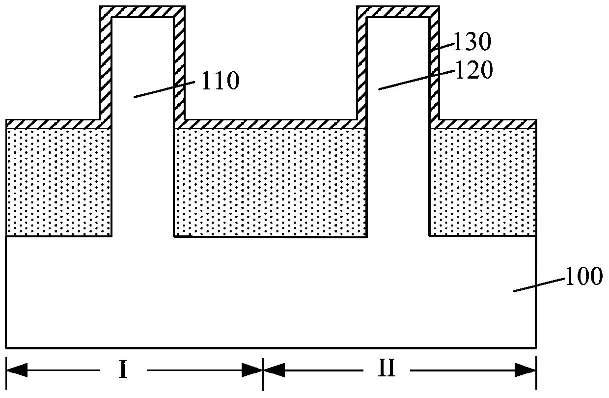
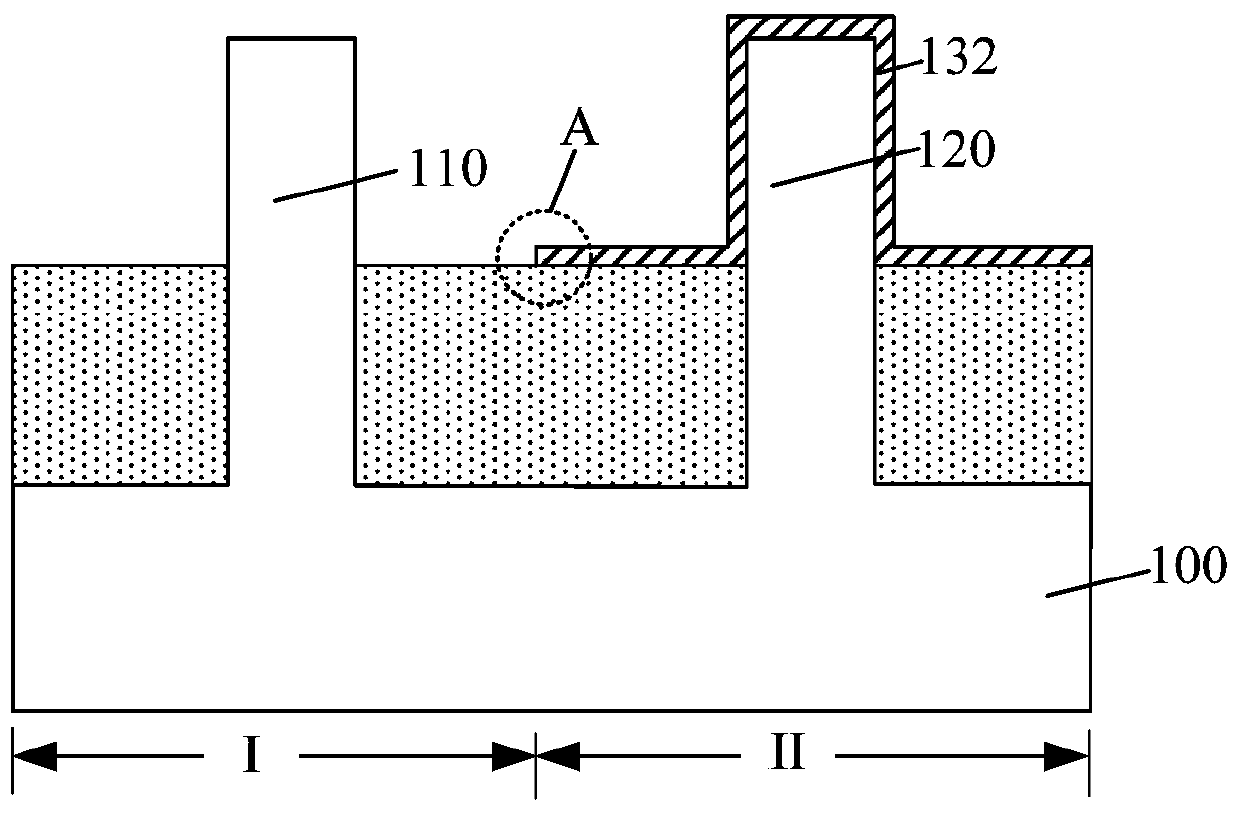
[0037] refer to Figure 1 to Figure 4 , shows a schematic structural diagram corresponding to each step in a manufacturing method of a semiconductor structure.

[0038] refer to figure 1, providing a base (not marked), the base includes a substrate 100 and a fin (not marked) protruding from the substrate 100 , the substrate 100 includes an NMOS region I and a PMOS region II. The NMOS region I is used to form a pull-down (PD, Pull Down) transistor, and the PMOS region II is used to form a pull-up (PU, Pull Up) transistor.

[0039] Specifically, the fin located in the NMOS region I is the first fin 110 , and the fin located in the PMOS region II is the second fin 120 .

[0040] refer to figure 2 , forming a P-type work function film 130 covering the ...


PUM


Abstract

A semiconductor structure and its manufacturing method, which include: provides a base, the base includes the foundation of the substrate, and the fins that are protruding on the substrate.It is used to form different types of transistors; forming a grid layer covering the top of the fins and side walls; a blocking layer on the gate layer at the junction of the first and second regions, andGallery medium layer; the secondary function layer is formed on the barricine layer and blocking layer in the second area; the first function layer layer is formed on the gate layer in the first region.The invention first forms a blocking layer on the gate layer at the junction of the first and second regions, and the blocking layer covers at least the barrier layer in the second region at the junction.The degree of diffusion of metal ions in the secondary function layer can avoid adverse effects on the performance of the secondary function layer.

Description

technical field [0001] The invention relates to the field of semiconductors, in particular to a semiconductor structure and a manufacturing method thereof. Background technique [0002] In the current semiconductor industry, integrated circuit products can be mainly divided into three types: logic, memory and analog circuits, among which memory devices account for a considerable proportion of integrated circuit products. With the development of storage technology, various types of semiconductor memories have appeared, such as Static Random Access Memory (SRAM, Static Random Access Memory), Dynamic Random Access Memory (DRAM, Dynamic Random Access Memory), Erasable Programmable Read-Only Memory ( EPROM, Erasable Programmable Read-Only Memory), Electrically Erasable Programmable Read-Only Memory (EEPROM, Electrically Erasable Programmable Read-Only) and flash memory (Flash). Since the SRAM has the advantages of low power consumption and fast working speed, more and more atten...

Claims


Application Information

Patent Timeline
Patent Type & Authority Patents(China)
IPC IPC(8): H01L27/11H01L27/092H01L21/8238H01L21/8244
CPCH01L27/0924H01L21/823821H01L21/823842H10B10/12
Inventor 周飞
Owner SEMICON MFG INT (SHANGHAI) CORP
Why Eureka
Try Eureka