A Low Offset Operational Amplifier Based on Regulation Active Load

An operational amplifier and active load technology, applied in the field of CMOS process integrated circuits, can solve problems such as operational amplifier offset

Active Publication Date: 2020-07-07
西安华泰半导体科技有限公司
View PDF8 Cites 0 Cited by
  • Summary
  • Abstract
  • Description
  • Claims
  • Application Information

AI Technical Summary

Problems solved by technology

[0004] The object of the present invention is to provide a low-offset operational amplifier based on regulating active loads to solve the problem of operational amplifier offset

Method used


Image

  • A Low Offset Operational Amplifier Based on Regulation Active Load
  • A Low Offset Operational Amplifier Based on Regulation Active Load
  • A Low Offset Operational Amplifier Based on Regulation Active Load

Examples


Embodiment 1

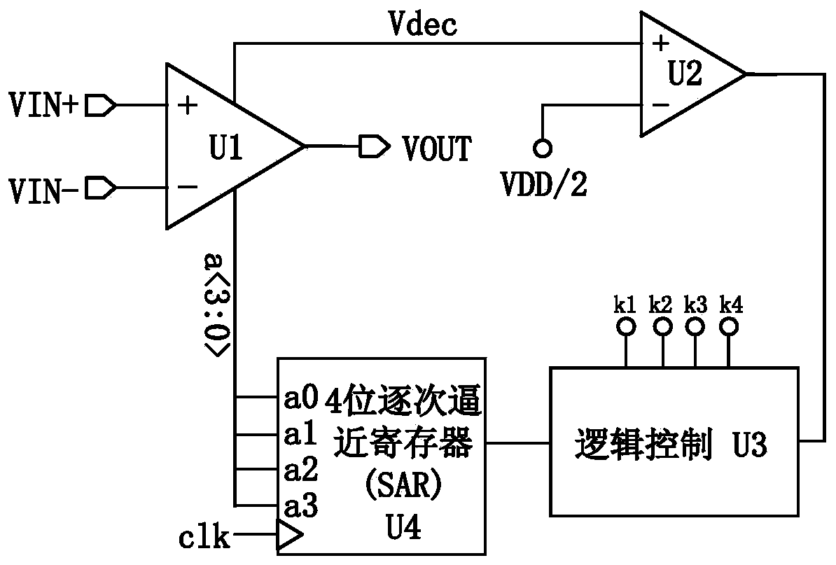
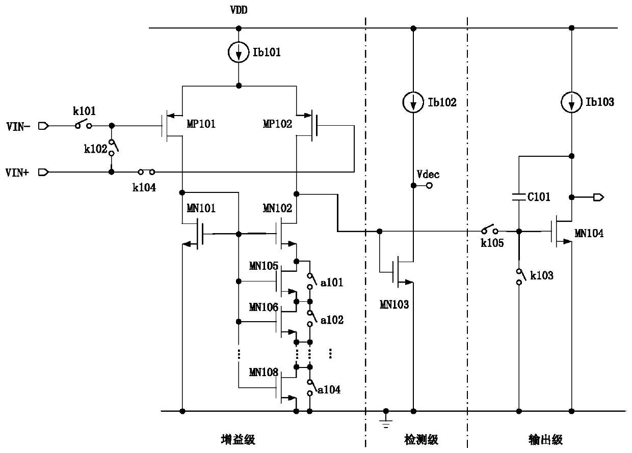
[0023] see figure 2 , The operational amplifier is divided into three parts: gain stage, detection stage, and output stage.

[0024] The gain stage includes: PMOS transistor MP101, PMOS transistor MP102, NMOS transistor MN101, NMOS transistor MN102, NMOS transistor MN105, NMOS transistor MN106, NMOS transistor MN107, NMOS transistor MN108, current source Ib101, switch k101, switch k102, switch k104, switch a101, switch a102, switch a103, switch a104. The non-inverting input terminal is connected to the gate of the PMOS transistor MP102 through k104, the inverting input terminal is connected to the gate of the PMOS transistor MP101 through k101, one terminal of the switch k102 is connected to the non-inverting input terminal, and the other terminal is connected to the gate of the PMOS transistor MP101. The PMOS transistor MP101 and the PMOS transistor MP102 are input tubes of the operational amplifier, and their sources are connected to one end of the bias current source Ib10...

Embodiment 2

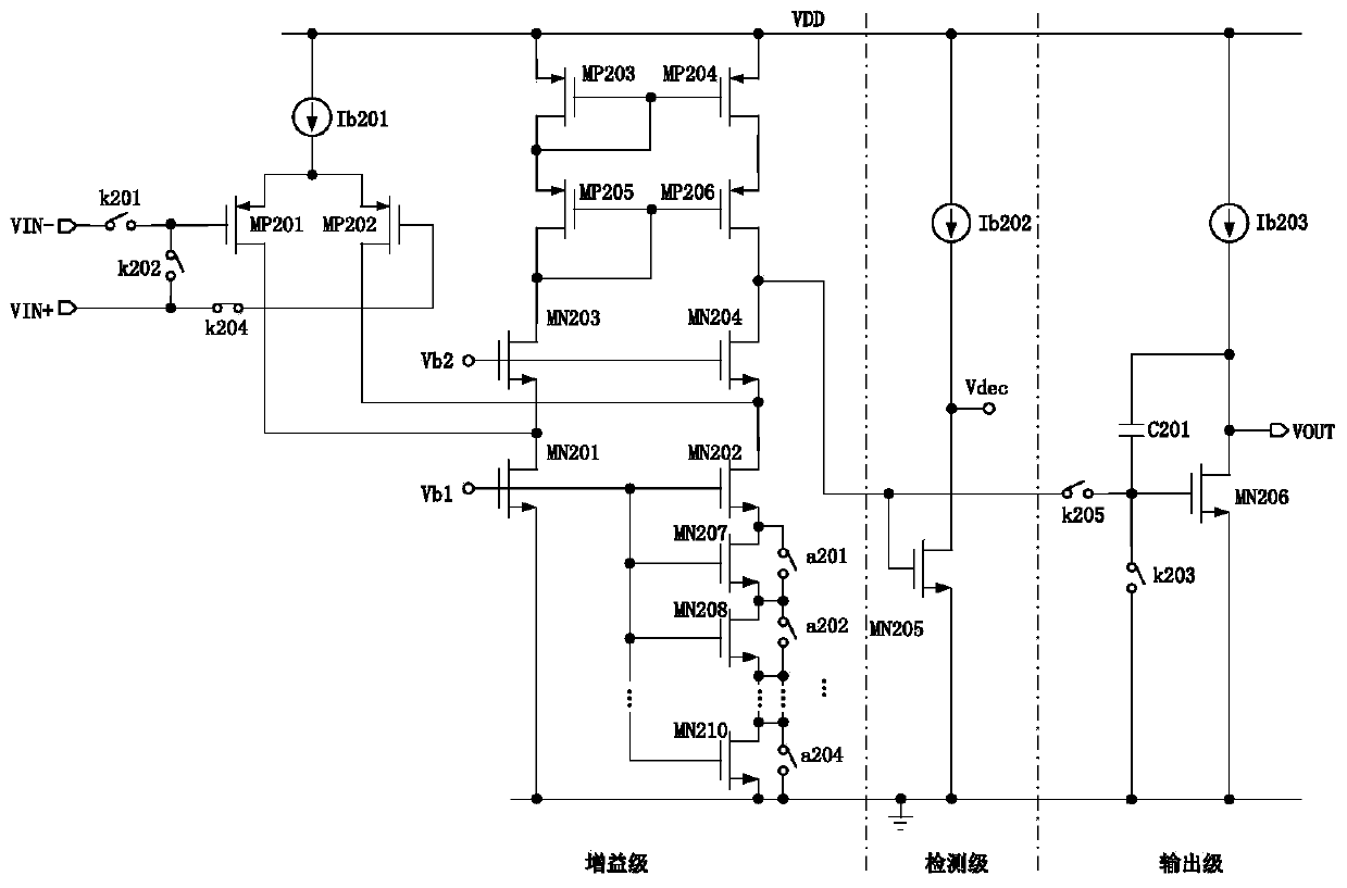
[0035] The structure of the operational amplifier in this embodiment is the same as that in Embodiment 1, and the gain stage in the main module of the operational amplifier is replaced by a folded cascode amplifier.

[0036] see figure 2 , the gain stage includes: PMOS transistor MP201, PMOS transistor MP202, PMOS transistor MP203, PMOS transistor MP204, PMOS transistor MP205, PMOS transistor MP206, NMOS transistor MN201, NMOS transistor MN202, NMOS transistor MN203, NMOS transistor MN204, NMOS transistor MN207, NMOS Transistor MN208, NMOS transistor MN209, NMOS transistor MN210, current source Ib201, switch k201, switch k202, switch k204, switch a201, switch a202, switch a203, switch a204. The non-inverting input terminal is connected to the gate of the PMOS transistor MP202 through k204, and the inverting input terminal is connected to the gate of the PMOS transistor MP201 through k201. One end of the switch k202 is connected to the non-inverting input end, and the other e...


PUM


Abstract

The invention discloses a low-offset operational amplifier based on regulation on active load, which comprises an operational amplifier module, a comparator module, a logic controlling unit and a four-site successive approaching register. The in-phase input end of the comparator module is connected with the detection voltage Vdec of the operational amplifier module, the antiphase input end of the comparator module is connected with VDD / 2, and the input end of the logic controlling unit is connected with the output end of the comparator module; the four-site successive approaching register is connected with the output end of the logic controlling unit and has four ports of a0, a1, a2 and a3 which are used for adjusting the number of transistors in in series connection with one side of the active load. According to the low-offset operational amplifier of the invention, the detection is added into the design, the uncertain jumping change of level at the output end to influence the use of a user when correcting the offset can be avoided.

Description

technical field [0001] The invention belongs to the field of CMOS process integrated circuits, and in particular relates to a low offset operational amplifier based on adjusting active loads. Background technique [0002] Due to the uncertainty of each process in the integrated circuit manufacturing process, the prepared operational amplifier inevitably has the problem of offset voltage. The offset voltage of the operational amplifier designed with bipolar transistor technology can achieve a relatively ideal effect, but bipolar transistor devices have large power consumption and high cost, so they are rarely used. Today's mainstream production technology is CMOS technology, which has the characteristics of low cost, low power consumption and high integration. However, the operational amplifier designed based on CMOS technology has a typical offset value of about 10mV, which cannot be tolerated in many applications. The offset voltage of the operational amplifier has two co...

Claims


Application Information

Patent Timeline
Patent Type & Authority Patents(China)
IPC IPC(8): H03F1/34H03F3/45H03G1/00H03G3/30
CPCH03F1/342H03F3/45179H03F2200/471H03F2203/45031H03F2203/45044H03G1/0088H03G3/30
Inventor 王红义朱奥麟徐延超周罡曹灿
Owner 西安华泰半导体科技有限公司
Why Eureka
Try Eureka