Eutectic soldering process method of microwave chip
A technology of eutectic welding and microwave chips, which is applied in the manufacture of electrical components, electrical solid devices, semiconductor/solid devices, etc., can solve the problems of not being suitable for the production of small batches, multi-variety modules, and high purchase costs
- Summary
- Abstract
- Description
- Claims
- Application Information
AI Technical Summary
Problems solved by technology
Method used
Image
Examples
Embodiment 1
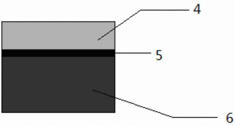
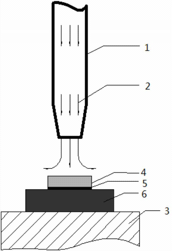
[0054]as attached figure 2 shown, with figure 2 It is a schematic diagram of microwave chip eutectic, carrier size specification: 4*8*0.2mm, preform size specification: 4*3.2*0.0254mm, chip size specification: 4*3.2*0.10mm; attached image 3 It is a schematic diagram of the microwave chip eutectic bonding process in Example 1. The specific implementation steps are as follows:
[0055] Step 1. Cleaning and drying of the carrier: put the carrier into an anhydrous ethanol solution, soak for 10 minutes, and then wipe the surface of the carrier (welding surface) with an absorbent cotton ball; then put the carrier into an oven at a temperature of 80-100°C , bake for 10 minutes;
[0056] Step 2. Plasma cleaning of the carrier: put the carrier in the previous step into a plasma cleaning machine for cleaning, and use argon gas for cleaning. The plasma cleaning power is: 500W, and the time: 15 minutes.
[0057] Step 3. Set the eutectic welding parameters:
[0058] The welding par...
PUM
 Abstract
Description
Claims
Application Information
 - R&D
- Intellectual Property
- Life Sciences
- Materials
- Tech Scout
- Unparalleled Data Quality
- Higher Quality Content
- 60% Fewer Hallucinations
Browse by: Latest US Patents, China's latest patents, Technical Efficacy Thesaurus, Application Domain, Technology Topic, Popular Technical Reports.
© 2025 PatSnap. All rights reserved.Legal|Privacy policy|Modern Slavery Act Transparency Statement|Sitemap|About US| Contact US: help@patsnap.com


