A shielded gate vdmos device with limited avalanche breakdown point

An avalanche breakdown and shielded gate technology, applied in semiconductor devices, electrical components, circuits, etc., can solve problems such as reducing parasitic BJT base resistance, increasing the threshold voltage of DMOS devices, and unable to completely prevent parasitic BJT transistors from turning on. The effect of improving withstand voltage and improving reliability

Active Publication Date: 2020-05-26
UNIV OF ELECTRONICS SCI & TECH OF CHINA
View PDF2 Cites 0 Cited by
  • Summary
  • Abstract
  • Description
  • Claims
  • Application Information

AI Technical Summary

Problems solved by technology

Similarly, such a solution still cannot completely eliminate the opening of the parasitic BJT tube, and it cannot completely avoid the device failure problem caused by avalanche breakdown; in addition, it cannot reduce the power DMOS through high-energy boron implantation or deep diffusion. The resistance of the P-body region under the N+ source region can be used to infinitely reduce the parasitic BJT base region resistance, because this will increase the threshold voltage (channel turn-on voltage) of the DMOS device

Method used


Image

  • A shielded gate vdmos device with limited avalanche breakdown point
  • A shielded gate vdmos device with limited avalanche breakdown point
  • A shielded gate vdmos device with limited avalanche breakdown point

Examples


Embodiment 1

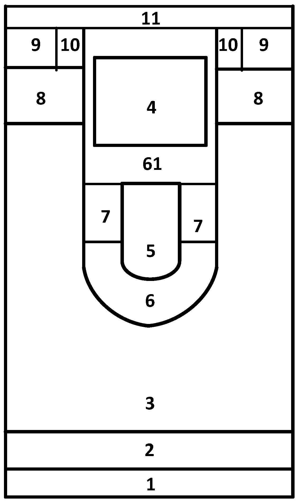
[0019] A shielded gate VDMOS device with a defined avalanche breakdown point, such as figure 1 As shown, it includes a metallized drain 1, a first conductive type semiconductor doped substrate 2, a first conductive type semiconductor doped drift region 3 and a metallized source 11 that are stacked sequentially from bottom to top; Type semiconductor doped drift region 3 has a groove gate, the second conductivity type semiconductor body region 8 is located on both sides of the groove gate and is in direct contact with the groove gate; the upper part of the second conductivity type semiconductor body region 8 has a second conductivity type semiconductor The doping contact region 9 and the first conductivity type semiconductor doping source region 10; the upper surface of the first conductivity type semiconductor doping source region 10 is in contact with the metallized source 11; the second conductivity type semiconductor doping contact The upper surface of the region 9 is in con...

Embodiment 2

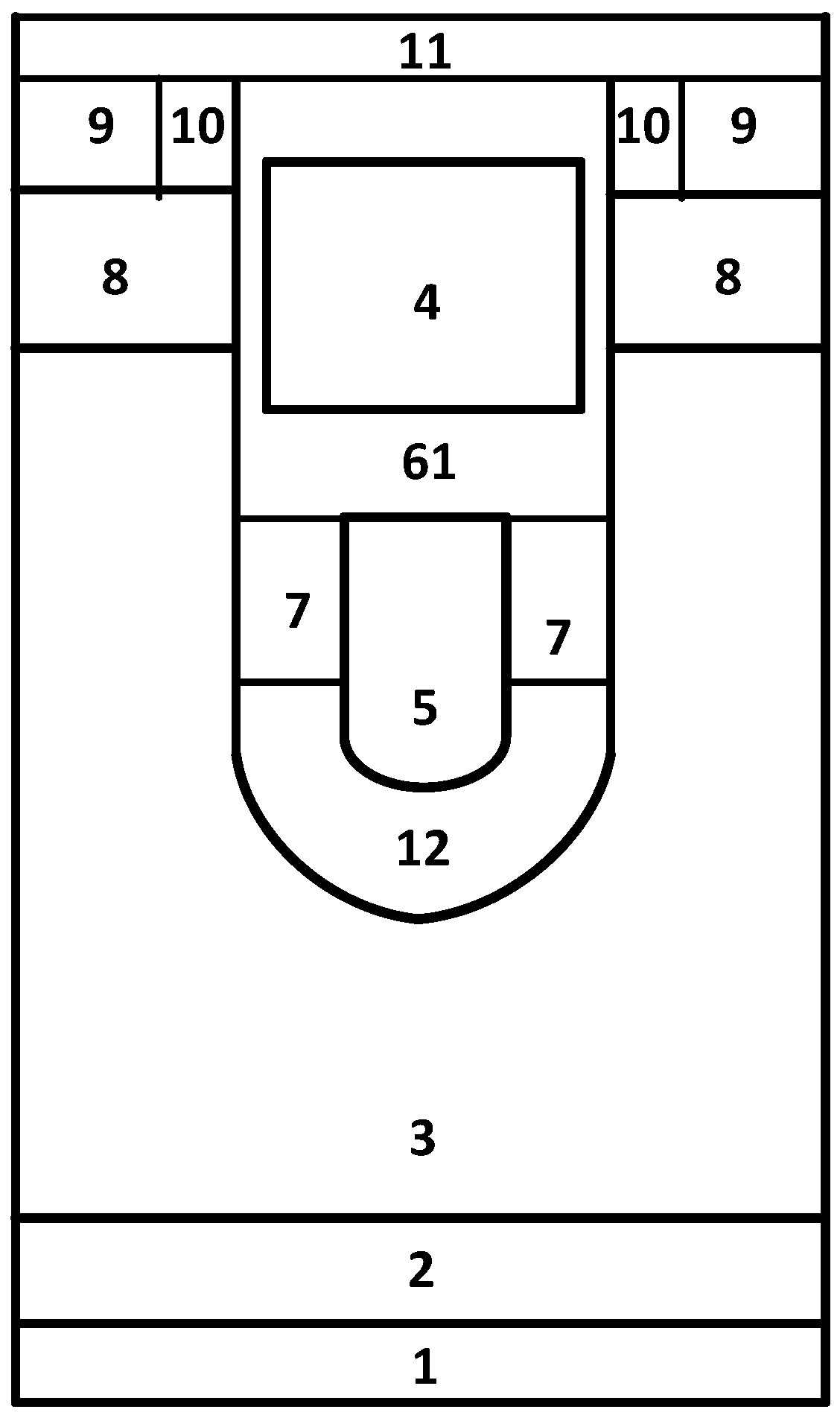
[0025] Such as image 3 As shown, the structure of this example is based on Example 1, the first dielectric layer 6 is replaced by a fourth dielectric layer 12, and the fourth dielectric layer 12 is made of a low-K dielectric material. That is, the dielectric constant of the material used in the second dielectric layer 7 is greater than that of the material used in the third dielectric layer 61, and the dielectric constant of the material used in the third dielectric layer 61 is greater than that of the material used in the fourth dielectric layer 12. The dielectric constant of the material. A low-K dielectric layer is used at the bottom of the trench gate, which can further improve the withstand voltage of the device.

Embodiment 3

[0027] Such as Figure 4 As shown, the structure of this example is based on Embodiment 1, the first dielectric layer 6 is replaced by a fourth dielectric layer 12, and the fourth dielectric layer 12 is made of a low-K dielectric material; the third dielectric layer 61 The fifth dielectric layer 13 is used instead, and the fifth dielectric layer 13 is made of a high-K dielectric material with a lower dielectric constant than the second dielectric layer 7 . That is, the dielectric constant of the material used in the second dielectric layer 7 is greater than the dielectric constant of the material used in the fifth dielectric layer 13, and the dielectric constant of the material used in the fifth dielectric layer 13 is greater than that of the material used in the fourth dielectric layer 12. the dielectric constant. A low-K dielectric layer is used at the bottom of the trench gate, which can further improve the withstand voltage of the device. The control gate electrode 4 is ...


PUM


Abstract

The invention relates to the technical field of power semiconductor devices, in particular to a shielded gate VDMOS device. The invention provides a shielded gate VDMOS device with limited avalanche breakdown point. In the existing shielded gate VDMOS device, by using different trench gate dielectric materials, electric field peaks are generated at the junction of different dielectric materials, so that the electric field peaks appear in the trenches of the middle. It not only prevents avalanche breakdown from occurring at the bottom of the groove, reducing the withstand voltage of the device, but also prevents avalanche breakdown from occurring at the top of the groove, reducing the UIS capability of the device. A shielded gate VDMOS device with a limited avalanche breakdown point proposed by the present invention not only improves the withstand voltage of the shielded gate VDMOS device, but also improves the shielded gate VDMOS device in the condition of basically not affecting other performances of the shielded gate VDMOS device. The reliability (that is, the ability to resist UIS failure) in the application of unclamped inductive loads makes a good compromise between UIS capability and withstand voltage of shielded gate VDMOS devices.

Description

technical field [0001] The invention belongs to the technical field of power semiconductors and relates to a shielded gate VDMOS device. Background technique [0002] In order to improve the performance of DMOS, new structures such as floating island unipolar devices and split-gates have been proposed at home and abroad. The floating island unipolar device increases the P-type voltage divider island in the N- epitaxial layer, so that the maximum electric field in the drift region is divided into two parts. Under the same doping concentration of the epitaxial layer, the breakdown voltage can be increased. The shielded gate VDMOS can use its first polycrystalline layer (Shield) as an "internal field plate" to reduce the electric field in the drift region, so the shielded gate VDMOS usually has lower on-resistance and higher breakdown voltage. [0003] The switching process under the unclamped inductive load (Unclamped Inductive Switching, UIS) is generally considered to be th...

Claims


Application Information

Patent Timeline
Patent Type & Authority Patents(China)
IPC IPC(8): H01L29/78H01L29/51
CPCH01L29/512H01L29/7813H01L29/407
Inventor 任敏罗蕾林育赐李佳驹谢驰李泽宏张波
Owner UNIV OF ELECTRONICS SCI & TECH OF CHINA
Why Eureka
Try Eureka