A hemt array electronically controlled terahertz wave modulator with network dislocation distribution
A dislocation distribution, terahertz wave technology, applied in instruments, nonlinear optics, optics, etc., to achieve the effect of enhancing resonance strength, improving terahertz wave transmittance, and simple structure
- Summary
- Abstract
- Description
- Claims
- Application Information
AI Technical Summary
Problems solved by technology
Method used
Image
Examples
Embodiment Construction
[0035] The present invention will be described in more detail below in conjunction with the accompanying drawings and examples.
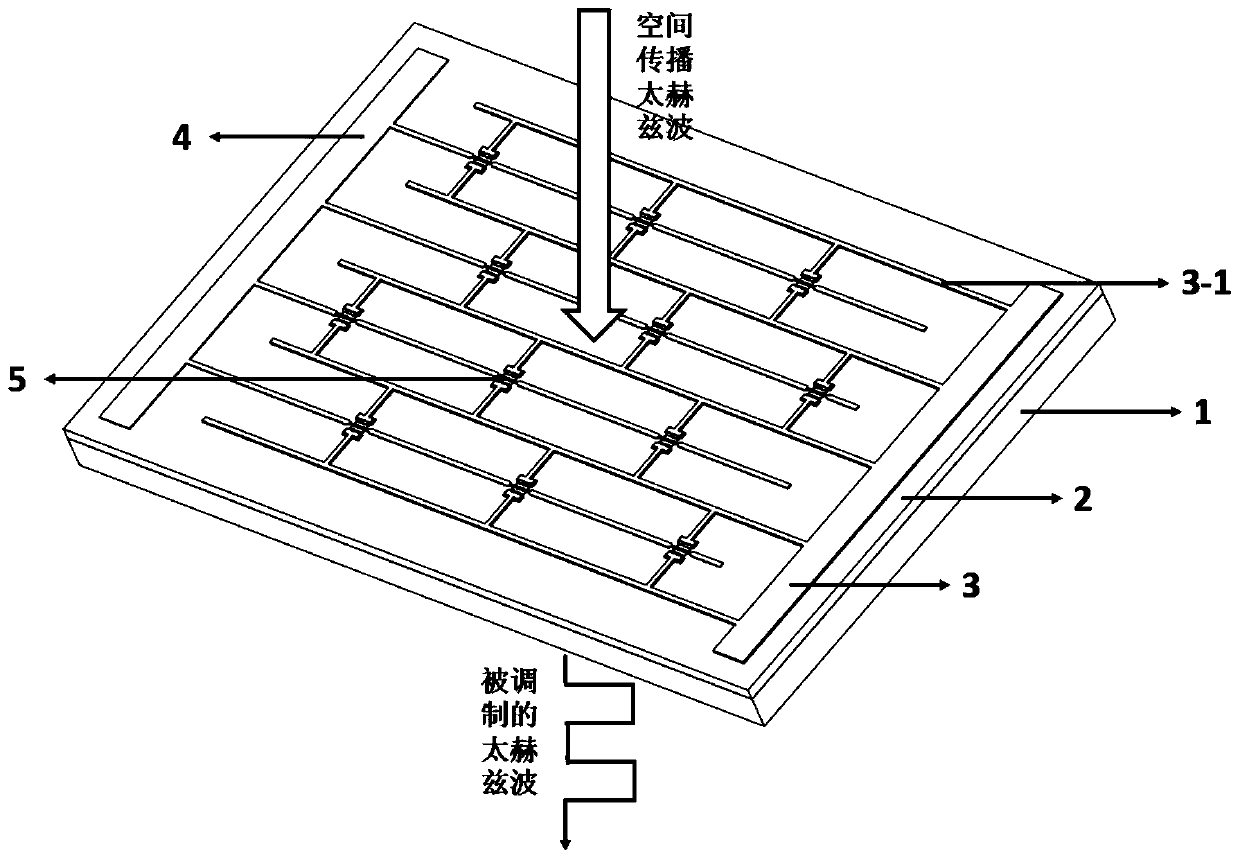
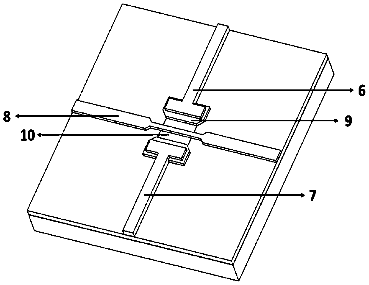
[0036] This specific embodiment provides a HEMT array electronically controlled terahertz wave modulator with network dislocation distribution, its structure is as follows figure 1As shown, it includes a semiconductor substrate 1 , a heterostructure epitaxial layer 2 , a modulation cell array 5 , a positive voltage loading electrode 3 and a negative voltage loading electrode 4 . The positive voltage loading electrode 3, the negative voltage loading electrode 4 and the modulation unit array 5 constitute a metal structure layer, and the lower surface of the metal structure layer is provided with a heterostructure epitaxial layer 2 and a semiconductor substrate 1 in sequence. The modulation unit array 5 is an M×N array composed of a plurality of modulation units, where M≥3 and N≥4. The modulation unit includes a HEMT and a metal resonant structure, an...
PUM
 Abstract
Description
Claims
Application Information
 - R&D
- Intellectual Property
- Life Sciences
- Materials
- Tech Scout
- Unparalleled Data Quality
- Higher Quality Content
- 60% Fewer Hallucinations
Browse by: Latest US Patents, China's latest patents, Technical Efficacy Thesaurus, Application Domain, Technology Topic, Popular Technical Reports.
© 2025 PatSnap. All rights reserved.Legal|Privacy policy|Modern Slavery Act Transparency Statement|Sitemap|About US| Contact US: help@patsnap.com


