
Rb-sic optical component polishing process processing method

A technology for optical components and process processing, applied in optical surface grinders, metal processing equipment, grinding/polishing equipment, etc., which can solve the problems of long cycle, low magnetron sputtering deposition rate, and film roughness deterioration.

Active Publication Date: 2018-10-30
XIAN TECH UNIV
View PDF1 Cites 0 Cited by
  • Summary
  • Abstract
  • Description
  • Claims
  • Application Information

AI Technical Summary

Problems solved by technology

[0011] The existing traditional optical processing methods have the following problems. First, the processing efficiency is low and the cycle time is long. Second, it is difficult to achieve an ultra-smooth surface (roughness RMS less than 1nm, surface shape RMS below λ / 5)
This is because: the deposition rate of magnetron sputtering is not high, and the deposition of tens of microns thick Si layer results in longer processing time. Second, magnetron sputtering deposits Si thin films. The roughness will deteriorate, usually from 7~8nm to more than ten nanometers

Method used


Image

  • Rb-sic optical component polishing process processing method
  • Rb-sic optical component polishing process processing method
  • Rb-sic optical component polishing process processing method

Examples


Embodiment 1

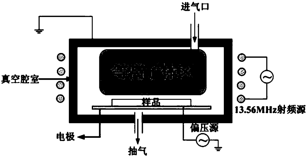
[0064] 1) ICP etching: see figure 2 , The background vacuum of the vacuum chamber of the ICP etching equipment is 2.0×10 -4 Pa, the working vacuum is controlled at 0.5~10Pa. Put the reaction sintered silicon carbide sample (RMS at 209.72nm) with a diameter of 150mm and a thickness of 10mm on the base of the vacuum chamber of the ICP etching equipment, and open the pre-pumping valve and the front-stage valve in sequence. When the pressure value of the composite vacuum gauge drops to At 5Pa, turn on the molecular pump, press the start button, wait until the molecular pump speed reaches 400r / min, open the high valve, and close the pre-pumping valve at the same time, when the pressure value of the composite vacuum gauge is lower than 10 -1 At Pa, set the gas flow meter to CF 4 Turn the switch of the gas flowmeter to the valve control position, adjust the knob of the flowmeter, set the flow rates of the two gases to 25sccm respectively, then open the main gas valve, adjust the h...


PUM

PropertyMeasurementUnit
surface roughnessaaaaaaaaaa

Abstract

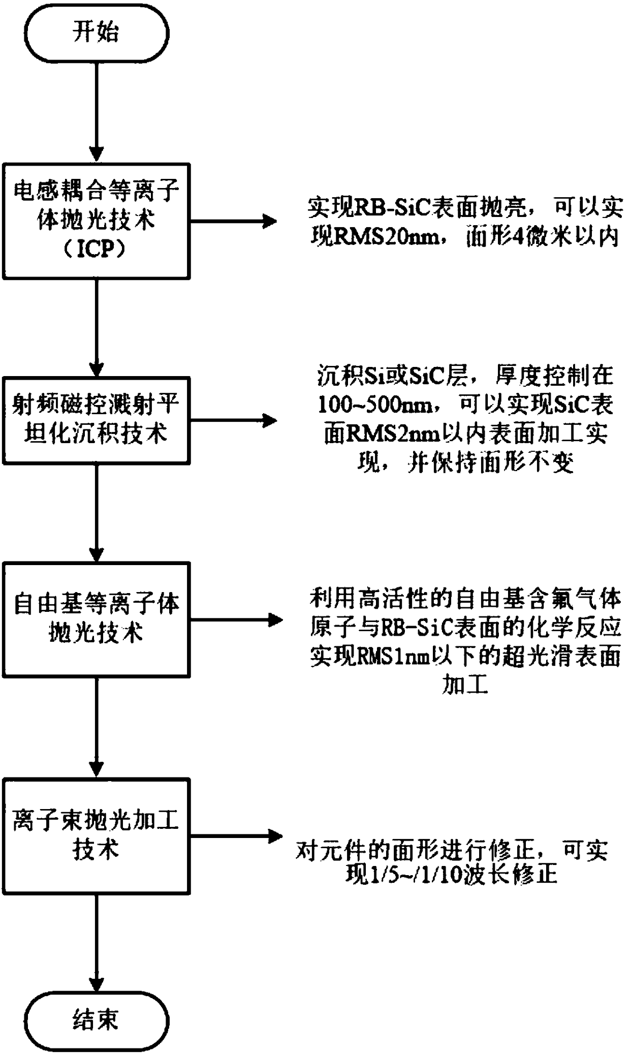
The invention discloses a machining method for the polishing process of an RB-SiC optical element. The machining method for the polishing process of the RB-SiC optical element comprises the steps that fine-grinding polishing of the RB-SiC optical element is achieved through the inductive coupling plasma polishing technique firstly, then a planarized nano-layer is deposited on the optical surface through the radio frequency magnetron sputtering surface planarization technique, and finally ultra-smooth surface machining of the optical element is achieved through the ion beam polishing shape-correction technique with the assistance of the free-radical microwave plasma polishing technique. Compared with the prior art, the plasma polishing technique is adopted by the novel machining method for polishing the RB-SiC optical element to replace a traditional optical machining method, the preparation technique of the planarized nano-layer and the ion beam shape-correction polishing technique are combined, the machining cycle of the large-diameter RB-SiC optical element is greatly shortened, and machining method for the polishing process of the RB-SiC optical element has the characteristics of high efficiency, high precision and low loss.

Description

technical field [0001] The present invention relates to the technical field of ultra-smooth precision machining on the surface of optical elements, in particular to a polishing process method for RB-SiC optical elements. Background technique [0002] In recent years, with the vigorous development of the aerospace industry and the rapid progress of social production, human beings have become more and more enthusiastic about exploring the space field. Aerospace technology has made significant contributions to human observation of space, research on the earth and the entire vast space. Many countries have begun to attach importance to the research of aerospace technology and space optics. In order to meet the requirements of use, large-scale space systems such as space telescopes and remote sensing reconnaissance cameras need to have a high enough resolution and a large enough aperture, but the increase of the aperture, the corresponding It will increase the weight of the entir...

Claims


Application Information

Patent Timeline
Patent Type & Authority Patents(China)
IPC IPC(8): B24B1/00B24B13/00
CPCB24B1/00B24B13/00
Inventor 惠迎雪刘卫国张进周顺徐均琪赵杨勇熊涛房沫岑
Owner XIAN TECH UNIV
Learn More