Method for preparing transparent copper thin film conductive electrode through replacement reaction via atomic layer deposition technology

An atomic layer deposition and displacement reaction technology, applied in coatings, circuits, photovoltaic power generation, etc., can solve problems such as the limitation of transparent conductive electrode substrates, poor light transmittance of metal film electrodes, and poor physical adhesion of conductive films. Control, good uniformity, excellent photoelectric performance

Inactive Publication Date: 2017-06-20
JILIN UNIV
View PDF5 Cites 2 Cited by
  • Summary
  • Abstract
  • Description
  • Claims
  • Application Information

AI Technical Summary

Problems solved by technology

Among them, the vacuum physical method mainly refers to the magnetron sputtering method, which can prepare dense and uniform transparent conductive films with good physical adhesion. poor
The chemical method is mainly the sol-gel method. The advantage of this method is that the production equipment is simple and it is easy to achieve uniform doping of multiple components, but the physical adhesion between the conductive film and the substrate is poor and the high temperature treatment limits the substrate of the transparent conductive electrode.

Method used


Image

  • Method for preparing transparent copper thin film conductive electrode through replacement reaction via atomic layer deposition technology
  • Method for preparing transparent copper thin film conductive electrode through replacement reaction via atomic layer deposition technology
  • Method for preparing transparent copper thin film conductive electrode through replacement reaction via atomic layer deposition technology

Examples


Embodiment 1

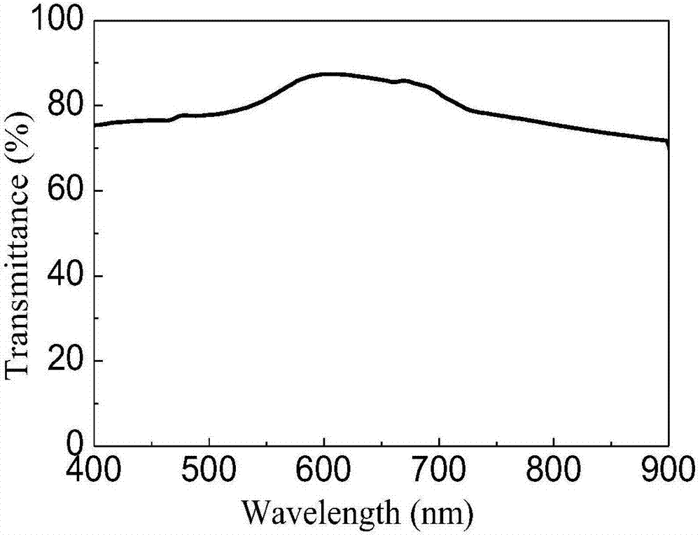
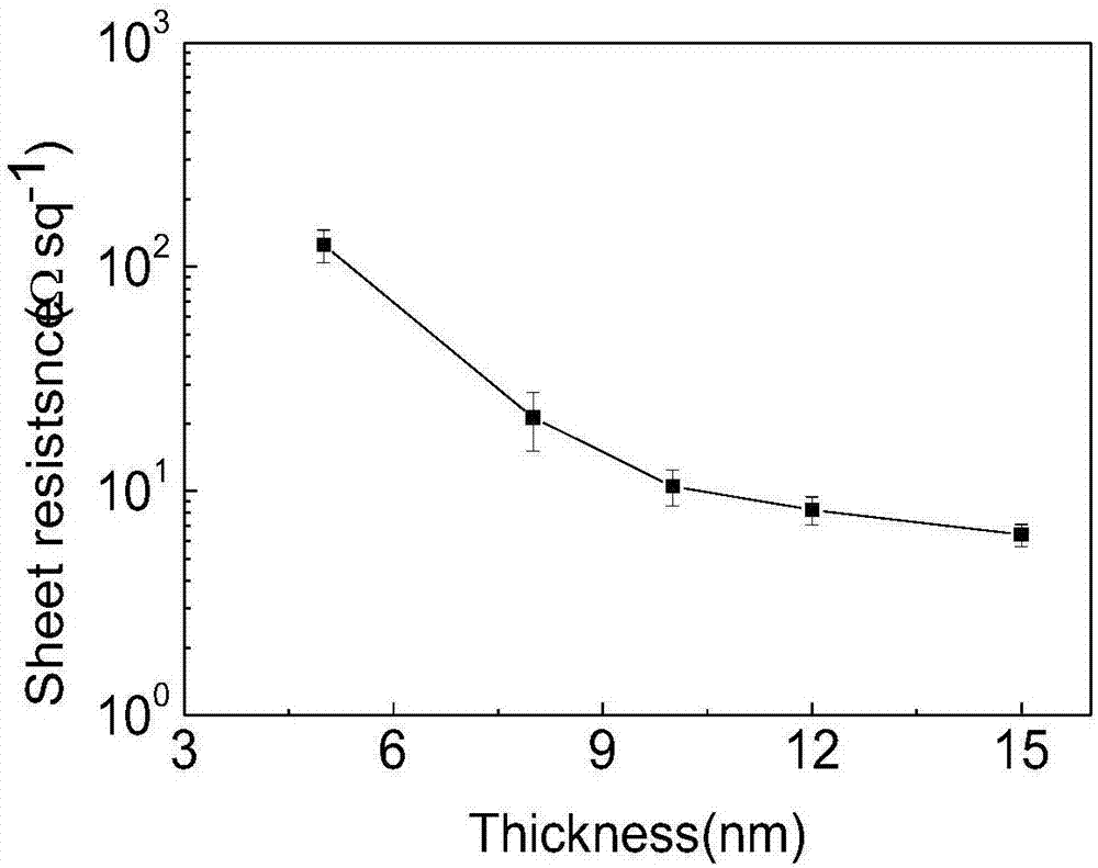
[0026] We prepared a sheet resistance as low as 6.2Ω / cm by atomic layer deposition through replacement reaction 2 , and the uniform transparent copper film conductive electrode with a light transmittance of about 80%.

[0027] The specific process is as follows:

[0028] 1) Wipe the 25×25mm glass substrate with acetone, ethanol and deionized water, then ultrasonically clean it with acetone, ethanol and deionized water, and then dry it with nitrogen;

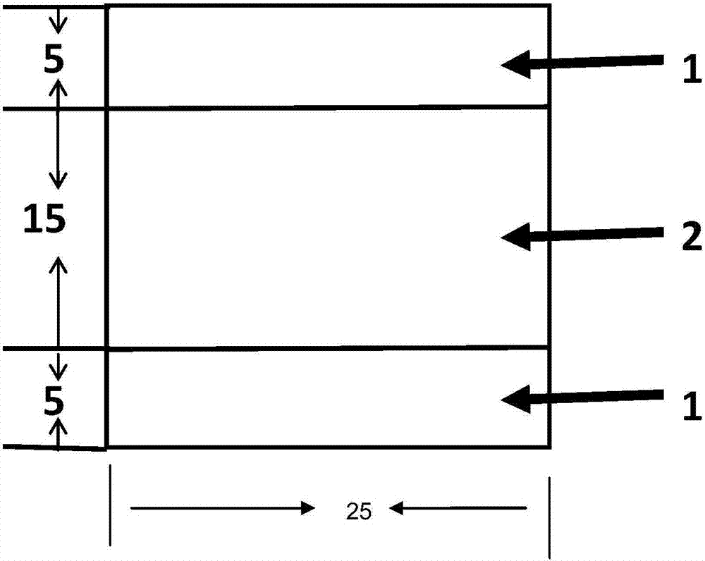
[0029] 2) Paste two separate silicon wafer protective films on the same side surface of the glass substrate cleaned in step 1), the structure and size of the protective film are as follows: figure 1 As shown, the upper and lower sides of the surface on the same side of the substrate are close to the edge of the protective film, its size is 25×5mm, and the middle part is the growth copper film area, its size is 25×15mm, and its function is to control the light-emitting area The area of ​​the anode and cathode contact short circu...

Embodiment 2

[0034]We used atomic layer deposition technology to prepare a 12nm (600 cycles) thick patterned uniform transparent copper thin film conductive electrode through the replacement reaction principle, and on this basis prepared a structure A: glass / ITO / HAT-CN (5nm) / TAPC(50nm) / Ir(ppy) 3 : CBP 5% (percent unit is molar weight) (15nm) / TPBI (30nm) / Liq (1nm) / Al and structure is B: glass / Cu (transparent copper thin film conductive electrode prepared by the present invention, 12nm) / HAT -CN(5nm) / TAPC(50nm) / Ir(ppy) 3 : CBP 5% (15nm) / TPBI (30nm) / Liq (1nm) / Al OLED device, wherein, HAT-CN is the hole injection layer, TAPC is the hole transport layer, Ir (ppy) 3 : CBP is the light-emitting layer, TPBI is the electron transport layer, Liq is the buffer layer, and Al is the cathode.

[0035] Among them, the ITO of the A group device is used as the OLED anode, and the 12nm transparent copper film conductive electrode of the B group device is used as the OLED anode. The specific process is as ...


PUM

PropertyMeasurementUnit
transmittivityaaaaaaaaaa

Abstract

The invention belongs to the technical field of transparent conductive electrode preparing, and relates to a method for preparing a transparent copper thin film conductive electrode through a replacement reaction via an atomic layer deposition technology. The method comprises the steps that firstly, a transparent substrate is subjected to cleaning treatment and then blow-dried through nitrogen; then, two separated protective films are pasted on the surface of the same side of the transparent substrate, the two protective films are symmetrically located at the positions, close to the edge, of the surface of the substrate, a graphical transparent substrate is obtained, and then the graphical transparent substrate is fed into a reaction chamber of atomic layer deposition equipment to carry out growth of a transparent copper thin film; and finally, the transparent substrate and the transparent copper thin film growing on the transparent substrate in a deposition manner are subjected to high-temperature annealing, the annealing temperature ranges from 200 DEG C to 300 DEG C, the annealing time ranges from 20 min to 30 min, and the graphical uniform transparent copper thin film conductive electrode is obtained on the transparent substrate. The transparent copper thin film conductive electrode prepared through the method is good in uniformity and excellent in photoelectric property and can be used for manufacturing solar cells, light-emitting diodes, LCDs, mobile phones and other photoelectric devices.

Description

technical field [0001] The invention belongs to the technical field of preparation of transparent conductive electrodes, and in particular relates to a method for preparing transparent copper thin film conductive electrodes through displacement reaction by using atomic layer deposition technology. Background technique [0002] Transparent conductive electrodes are widely used in flat panel displays, solid-state lighting, microdisplays, solar cells, and photodetectors, and are key components of optoelectronic devices. At present, the most commonly used film material for transparent conductive electrodes is the ITO film prepared on glass or other transparent substrates by magnetron sputtering technology. However, although the ITO film has relatively good light transmittance, its application also has many limitations, such as : a) The electrical conductivity is relatively poor; b) The indium required for the preparation of the ITO film is a rare metal, which is less in the eart...

Claims


Application Information

Patent Timeline
Patent Type & Authority Applications(China)
IPC IPC(8): C23C16/04C23C16/18C23C16/455H01L31/0224H01L33/36G02F1/1343
CPCC23C16/042C23C16/18C23C16/45553G02F1/13439H01L31/022425H01L33/36Y02E10/50
Inventor 段羽熊鹏鹏陈平刘云飞刘辉王浩然赵毅
Owner JILIN UNIV
Why Eureka
Try Eureka