High-quality gallium oxide wafer preparation method and application
A gallium oxide, high-quality technology, applied in semiconductor/solid-state device manufacturing, semiconductor devices, electrical components, etc., can solve the problems of small chip size, low chip quality, chip breakage, etc., to achieve stress relief, high chip quality, The effect of regulating resistivity
- Summary
- Abstract
- Description
- Claims
- Application Information
AI Technical Summary
Problems solved by technology
Method used
Image
Examples
Embodiment 1
[0044] A method for preparing a high-quality gallium oxide wafer, comprising the following steps:
[0045] (1) Bulk single crystal pretreatment
[0046] Cut the grown high-quality gallium oxide or doped gallium oxide single crystal into 7×5×3mm 3 For the sample, the larger surface of the sample is the (100) plane, and a bulk single crystal is obtained. The cut bulk single crystal is placed in an atmosphere furnace for annealing at an annealing temperature of 900° C. for 5 hours, and the atmosphere is flowing hydrogen.
[0047] (2) Mechanical peeling
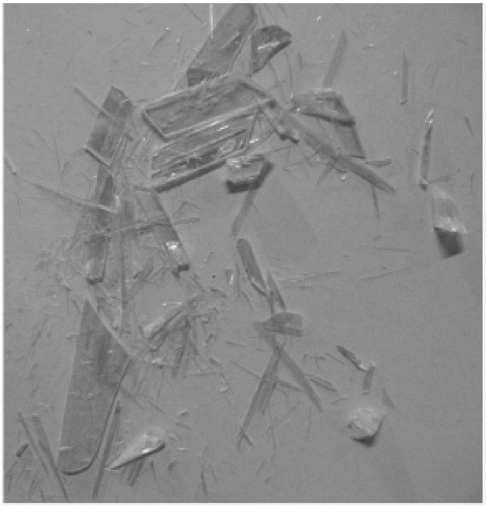
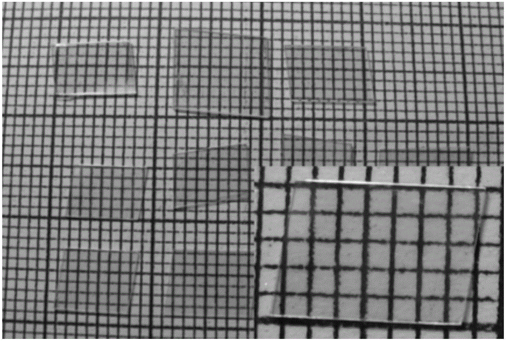
[0048] Scratch the side of the cut bulk single crystal with a diamond knife, put it in 25°C water, and then use a sharp blade to cut along the (100) plane from the scratch, and slowly separate the wafer from the bulk single crystal , to obtain high-quality gallium oxide wafers. Chip such as figure 2 shown. pass figure 2 It can be seen that the wafer obtained by mechanical peeling after pretreatment will not break, the wa...
Embodiment 2
[0052] A method for preparing a high-quality gallium oxide wafer, comprising the following steps:
[0053] (1) Bulk single crystal pretreatment
[0054] Cut the grown high-quality gallium oxide or doped gallium oxide single crystal into 10×6×3mm 3 For the sample, the larger surface of the sample is the (100) plane, and a bulk single crystal is obtained. The cut bulk single crystal is placed in an atmosphere furnace for annealing, the annealing temperature is 1000°C, the annealing time is 15h, and the atmosphere is flowing argon.
[0055] (2) Mechanical peeling
[0056] Scratch the side or edge of the annealed crystal with a diamond knife, put it into 20°C water, and then use a sharp blade to cut along the (100) plane from the scratch, and then slowly remove the wafer from the bulk A single crystal is separated to obtain a high-quality gallium oxide wafer.
Embodiment 3
[0058] A method for preparing a high-quality gallium oxide wafer, comprising the following steps:
[0059] (1) Bulk single crystal pretreatment
[0060] Cut the grown high-quality Sn-doped n-type gallium oxide single crystal into 25×20×3mm 3 For the sample, the larger surface of the sample is the (100) plane, and a bulk single crystal is obtained. The cut bulk single crystal is placed in an atmosphere furnace for annealing, the annealing temperature is 1000° C., the annealing time is 40 h, and the atmosphere is flowing argon.
[0061] (2) Mechanical peeling
[0062] Cut the bulk single crystal, use a diamond knife to scratch the side of the annealed crystal, put it in 28°C water, then use a sharp blade to cut along the (100) plane from the scratch, and then slowly remove the wafer from the bulk single crystal On separation, high-quality gallium oxide wafers are obtained.
[0063] (3) Wafer post-processing
[0064] The obtained wafer was annealed at 800° C. under argon for...
PUM
 Abstract
Description
Claims
Application Information
 - R&D
- Intellectual Property
- Life Sciences
- Materials
- Tech Scout
- Unparalleled Data Quality
- Higher Quality Content
- 60% Fewer Hallucinations
Browse by: Latest US Patents, China's latest patents, Technical Efficacy Thesaurus, Application Domain, Technology Topic, Popular Technical Reports.
© 2025 PatSnap. All rights reserved.Legal|Privacy policy|Modern Slavery Act Transparency Statement|Sitemap|About US| Contact US: help@patsnap.com


