Method for homoepitaxially growing gallium nitride, gallium nitride material and application thereof
A homoepitaxial and epitaxial growth technology, applied in the field of gallium nitride materials obtained by growth, can solve the problems of difficult epitaxial growth, high defect density, large grain boundaries, etc.
- Summary
- Abstract
- Description
- Claims
- Application Information
AI Technical Summary
Problems solved by technology
Method used
Image
Examples
preparation example Construction
[0041] In some embodiments, the preparation method of the gallium nitride material includes:
[0042] GaN substrates are provided;
[0043] setting a single layer of graphene as an insertion layer on the gallium nitride substrate;
[0044] GaN material is homoepitaxially grown on the substrate carrying the single-layer graphene.
[0045] In some embodiments, the preparation method of the gallium nitride material includes: transferring a single-layer graphene onto the substrate as the insertion layer; or directly growing a single-layer graphite on the substrate ene as the intercalation layer.
[0046] Preferably, the preparation method of the gallium nitride material comprises: epitaxially growing a low-temperature layer of gallium nitride on the substrate carrying the single-layer graphene, wherein the growth temperature used is 500-800°C, and then GaN materials are epitaxially grown at a high temperature of 1000-1100 °C.
[0047] Another aspect of the embodiments of the p...
Embodiment 1
[0051] 1. Use a gallium nitride template (4 micron thick gallium nitride grown on a sapphire substrate by MOCVD) as the substrate.
[0052] 2. Transfer or direct growth of single-layer graphene on GaN.
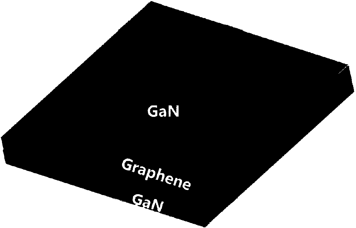
[0053] 3. Since gallium nitride will decompose at 850°C, MOCVD equipment is used to first grow the low-temperature layer of gallium nitride at a low temperature of 600°C, and the growth V / III is 3000 pure hydrogen as the carrier gas; then nitrogen is grown at a high temperature of 1040°C Gallium nitride, the growth V / III is 2000, pure hydrogen is used as the carrier gas, and the gallium nitride material is finally obtained after growth, please refer to figure 1 shown.
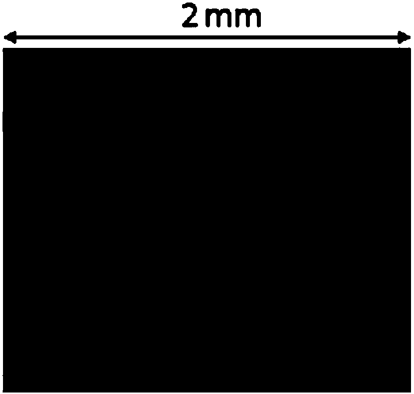
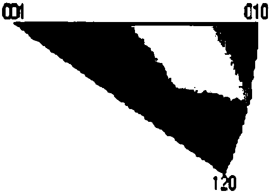
[0054] The gallium nitride material obtained in this embodiment is tested for performance and found that it is a single crystal material (see Figure 2a and Figure 2b shown), and aligned with the underlying GaN orientation. The single-layer graphene is only 3-5 angstroms at the gallium nitride interface, a...
Embodiment 2
[0056] 1. Use self-supporting gallium nitride (thickness of 350 micron gallium nitride) as the substrate.
[0057] 2. Transfer or direct growth of single-layer graphene on GaN.
[0058] 3. Since gallium nitride will decompose at 850°C, HVPE equipment is used to first grow the low-temperature layer of gallium nitride at a low temperature of 600°C, the growth V / III is 30, and the nitrogen-hydrogen ratio is 1:1 as the carrier gas; then Gallium nitride is grown at a high temperature of 1040°C, the growth V / III is 20, and the ratio of nitrogen to hydrogen is 1:1 as the carrier gas. After growth, gallium nitride material is finally obtained. Please refer tofigure 1 shown.
[0059] The gallium nitride material obtained in this embodiment is tested for performance and found that it is a single crystal material (see Figure 2a and Figure 2b shown), and aligned with the underlying GaN orientation. The single-layer graphene is only 3-5 angstroms at the gallium nitride interface, and ...
PUM
| Property | Measurement | Unit |
|---|---|---|
| thickness | aaaaa | aaaaa |
| thickness | aaaaa | aaaaa |
Abstract
Description
Claims
Application Information
 - Generate Ideas
- Intellectual Property
- Life Sciences
- Materials
- Tech Scout
- Unparalleled Data Quality
- Higher Quality Content
- 60% Fewer Hallucinations
Browse by: Latest US Patents, China's latest patents, Technical Efficacy Thesaurus, Application Domain, Technology Topic, Popular Technical Reports.
© 2025 PatSnap. All rights reserved.Legal|Privacy policy|Modern Slavery Act Transparency Statement|Sitemap|About US| Contact US: help@patsnap.com


