
Method for reducing effect of base plane dislocation on silicon carbide epitaxial layer

A silicon carbide and epitaxial layer technology, applied in the direction of semiconductor devices, electrical components, circuits, etc., can solve the problems of surface degradation of epitaxial materials, easy damage to the surface of the buffer layer, and fast etching rate of silicon carbide, so as to reduce the possibility and improve the Surface quality, damage reduction effect

Active Publication Date: 2017-05-24
NO 55 INST CHINA ELECTRONIC SCI & TECHNOLOGYGROUP CO LTD
View PDF2 Cites 13 Cited by
  • Summary
  • Abstract
  • Description
  • Claims
  • Application Information

AI Technical Summary

Problems solved by technology

However, during the high-temperature annealing process, due to the high temperature, the etching rate of hydrogen gas on silicon carbide is fast, and the surface of the buffer layer is easily damaged, resulting in the surface degradation of the epitaxial material that is subsequently grown. Therefore, this principle has not been applied to the epitaxial process.

Method used


Image

  • Method for reducing effect of base plane dislocation on silicon carbide epitaxial layer
  • Method for reducing effect of base plane dislocation on silicon carbide epitaxial layer

Examples


Embodiment Construction

[0019] The technical solutions of the present invention will be further described below in conjunction with the accompanying drawings and embodiments.

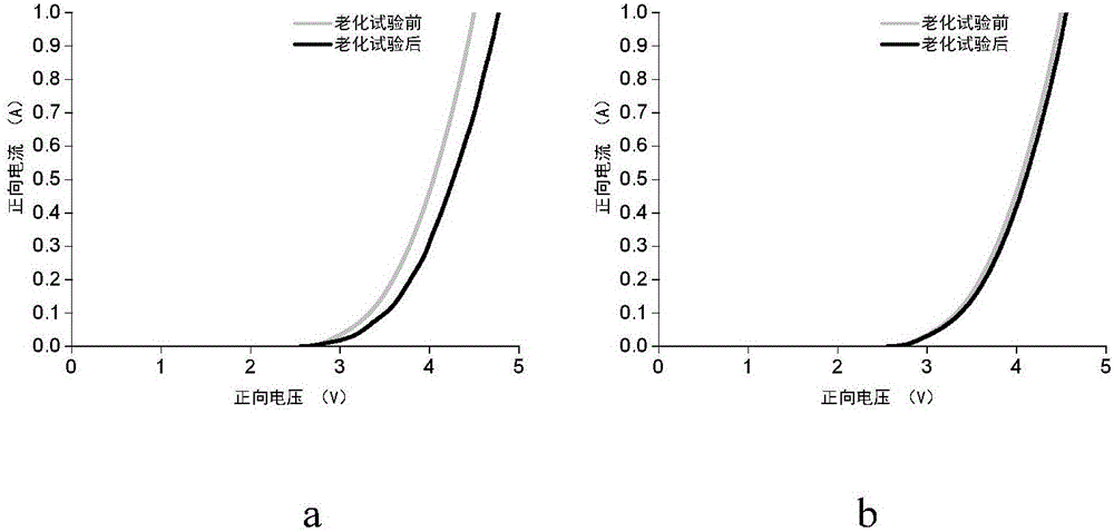
[0020] The method for reducing the influence of basal plane dislocations on the silicon carbide epitaxial layer described in the present invention, by reducing the flow rate of hydrogen gas during the high-temperature annealing process and increasing the pressure of the reaction chamber, suppresses the etching effect of hydrogen gas on the substrate, and completes the highly doped buffer layer. The high-temperature annealing treatment, and then continue to use the graded buffer layer grown at a low epitaxial rate, which can reduce the difference in doping concentration between the epitaxial layer and the high-doped buffer layer, and can improve the surface quality of the subsequent epitaxial layer. This epitaxial method can effectively reduce the epitaxial layer. The probability of stacking fault defects derived from basal plan...


PUM


Abstract

The invention discloses a method for reducing an effect of base plane dislocation on a silicon carbide epitaxial layer. The method comprises the steps of: carrying out interface high-temperature annealing processing on a silicon carbide substrate to promote a BPD-TED inversion point to move downward and away from a heavily-doped buffer layer surface; adding a gradient buffer layer to reduce a concentration difference between a heavily-doped buffer layer and the epitaxial layer, repairing a heavily-doped buffer layer interface etched by a high-temperature hydrogen gas; and performing surface etch pit repairing on the heavily-doped buffer layer by utilizing the feature of lateral epitaxial growth enhancement in a low-speed epitaxial mode, and improving surface quality of the subsequent epitaxial layer. The method can reduce the base plane dislocation inversion point below the heavily-doped buffer layer interface, effectively decreases the probability of deriving a stacking fault defect by base plane dislocation under the action of a high current in the epitaxial layer, and adopts the process compatible with the conventional epitaxial process.

Description

technical field [0001] The invention relates to a method for growing a silicon carbide epitaxial layer with high surface quality, in particular to a method for reducing the influence of basal plane dislocations on the silicon carbide epitaxial layer. Background technique [0002] Now the perfection of commercial silicon carbide substrate crystals has been greatly improved, but there are still a large number of basal plane dislocations (BPD) in the silicon carbide substrate, and the BPD may extend to the epitaxial layer, and under the action of the forward conduction current It evolves into a stacking fault (SF), which causes the forward voltage drift of the high-frequency diode device. Since edge dislocations (TED) have much less impact on device performance, increasing the ratio of BPD to TED during the epitaxial growth of silicon carbide and preventing BPD in the substrate from extending into the epitaxial layer are very important for improving device performance. importa...

Claims


Application Information

Patent Timeline
Patent Type & Authority Applications(China)
IPC IPC(8): H01L21/28
CPCH01L21/28185H01L21/02378H01L21/02447H01L21/02502H01L21/0251H01L21/02529H01L21/0262H01L21/02661H01L21/02123H01L21/02293H01L21/02436H01L21/02612H01L21/3065
Inventor 李赟
Owner NO 55 INST CHINA ELECTRONIC SCI & TECHNOLOGYGROUP CO LTD
Learn More