Cleaning method for texturing of poly-silicon wafer

A technology of polycrystalline silicon wafers and silicon wafers, applied in semiconductor/solid-state device manufacturing, photovoltaic power generation, electrical components, etc., can solve the problems of reducing reflectivity, large suede surface, increasing light absorption, etc., to achieve improved electrical performance and low reflectivity Effect

Active Publication Date: 2017-05-17
JETION SOLAR HLDG
View PDF2 Cites 8 Cited by
  • Summary
  • Abstract
  • Description
  • Claims
  • Application Information

AI Technical Summary

Problems solved by technology

Texturing is the first process for manufacturing crystalline silicon cells, also known as "surface texturing". The effective textured structure makes the incident light reflect and refract multiple times on the surface of the silicon wafer, increasing light absorption and reducing reflectivity , which helps to improve the performance of the battery. After the suede is prepared, the required suede is prepared by washing, alkali washing, water washing, pickling and other processes. However, during the alkali washing, the alkali will further corrode the silicon wafer. Since the crystal structure of polysilicon is an irregular crystal orientation, if all reactions are in the same crystal orientation, the brightness will be inconsistent with other crystal orientations. At this time, the reaction rate cannot be well controlled, resulting in a large suede surface when preparing the suede surface. and small suede case

Method used


Image

  • Cleaning method for texturing of poly-silicon wafer
  • Cleaning method for texturing of poly-silicon wafer

Examples


Embodiment Construction

[0026] Objects, advantages and features of the present invention will be illustrated and explained by the following non-limiting description of preferred embodiments. These embodiments are only typical examples of applying the technical solutions of the present invention, and all technical solutions formed by adopting equivalent replacements or equivalent transformations fall within the protection scope of the present invention.

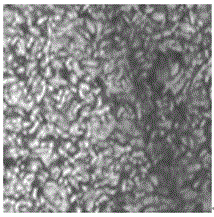
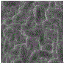
[0027] Silicon wafer texturing is a very important step in the processing of silicon solar cells. Texturing can not only form a textured surface with good light trapping properties, but also remove the damaged layer on the surface of the silicon wafer to form a textured surface that is good for the smoothness of the PN junction.

[0028] Such as figure 1 As shown, the present invention provides a kind of cleaning method of polycrystalline silicon chip texturing, the silicon chip after making texturing is cleaned, and this method comprises the followi...


PUM


Abstract

The invention discloses a cleaning method for texturing of a poly-silicon wafer. The cleaning method is used for cleaning the silicon wafer after being textured and comprises the following steps of S1, texturing with an acid; S2, washing the silicon wafer after being subjected to the step S1; S3, placing the silicon wafer after being washed in a first cleaning liquid for immersion and cleaning; S4, washing the silicon wafer after being cleaned by the first cleaning liquid; S5, placing the silicon wafer after being washed in the step S4 in a second cleaning liquid for immersion and cleaning; S6, washing the silicon wafer after being cleaned by the second cleaning liquid; S7, placing the silicon wafer after being washed in the step S6 in a third cleaning liquid for immersion and cleaning; and S8, drying the silicon wafer after being cleaned by the third cleaning liquid. By the cleaning method, the reaction of an alkali and the silicon wafer during the alkali cleaning process is obviously improved, an existing texturing surface is prevented from being damaged to form texturing equipment with lower reflectivity, so that the electrical property of a battery is improved.

Description

technical field [0001] The invention relates to the technical field of solar cell panel manufacturing, and more specifically, relates to a method for cleaning polycrystalline silicon chip texture. Background technique [0002] Photovoltaic power generation is a technology that directly converts light energy into electrical energy by using the photovoltaic effect of the semiconductor interface. It is one of the main ways to use solar energy at present. Photovoltaic power generation has no risk of depletion; safe and reliable, no noise, no pollution emissions In addition, it is absolutely clean (no pollution); it is not limited by the geographical distribution of resources, and the advantages of building roofs can be used; for example, areas without electricity, and areas with complex terrain; local power generation and power supply can be generated without consuming fuel and erecting transmission lines; energy With the advantages of high quality, it has become an emerging ind...

Claims


Application Information

Patent Timeline
Patent Type & Authority Applications(China)
IPC IPC(8): H01L21/02H01L31/0236
CPCH01L31/02366H01L21/02057Y02E10/50Y02P70/50
Inventor 曾石发
Owner JETION SOLAR HLDG
Why Eureka
Try Eureka