Electrostatic discharge protection structure

An electrostatic discharge protection and electrostatic discharge technology, applied in circuits, electrical components, electrical solid devices, etc., can solve the problems of latch-up effect and low maintenance voltage, and achieve the purpose of avoiding latch-up effect, increasing maintenance voltage, and not easily damaged. Effect

Active Publication Date: 2015-07-22
SEMICON MFG INT (SHANGHAI) CORP +1
View PDF5 Cites 0 Cited by
  • Summary
  • Abstract
  • Description
  • Claims
  • Application Information

AI Technical Summary

Problems solved by technology

[0006] The invention solves the problem that the existing electrostatic discharg...

Method used


Image

  • Electrostatic discharge protection structure
  • Electrostatic discharge protection structure
  • Electrostatic discharge protection structure

Examples


Embodiment Construction

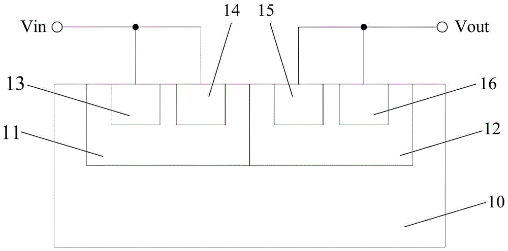
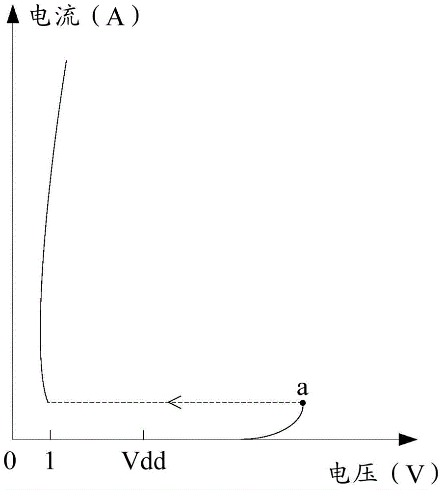
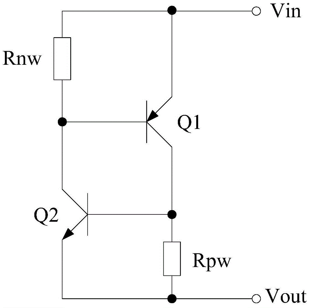
[0037] As described in the background art, figure 1 The holding voltage of the thyristor structure shown is relatively low, which may easily cause damage to the thyristor structure. image 3 yes figure 1 The equivalent circuit diagram of the thyristor structure shown, refer to image 3 , the thyristor structure includes a parasitic PNP transistor Q1, a parasitic NPN transistor Q2, a first parasitic resistor Rnw, and a second parasitic resistor Rpw. The emitter of the parasitic PNP transistor Q1 and one end of the first parasitic resistor Rnw are coupled to the electrostatic discharge input terminal Vin, and the base of the parasitic PNP transistor Q1 is connected to the other end of the first parasitic resistor Rnw and the The collector of the parasitic NPN transistor Q2, the collector of the parasitic PNP transistor Q1 is connected to the base of the parasitic NPN transistor Q2 and one end of the second parasitic resistor Rpw; the other end of the second parasitic resistor ...


PUM


Abstract

An electrostatic discharge protection structure comprises a P-type substrate, an N-type well region and a P-type well region located in the P-type substrate, a first N-type doping region and a first P-type doping region located in the N-type well region, a second N-type doping region and a second P-type doping region located in the P-type well region, and a counter doping region located in at least one well region, wherein the N-type well region and the P-type well region are adjacent and contacted; the first N-type doping region and the first P-type doping region are coupled with an electrostatic discharge input end; the second N-type doping region and the second P-type doping region are coupled with an electrostatic discharge output end; and the counter doping region is used for enhancing impedance between the electrostatic discharge input end and the electrostatic discharge output end. According to the electrostatic discharge protection structure provided by the technical scheme of the invention, the maintaining voltage is large, and latch-up effects can be avoided.

Description

technical field [0001] The invention relates to electrostatic discharge protection technology, in particular to an electrostatic discharge protection structure. Background technique [0002] With the increasing application of semiconductor chips, more and more semiconductor chips are damaged by static electricity. Generally, an electrostatic voltage of about 10V may damage semiconductor chips without electrostatic discharge (ESD, electrostatic discharge) protection. There are many designs and applications of electrostatic discharge protection structures, generally including: thin-gate N-type field effect transistors, diodes, Zener tubes, silicon controlled rectifier (SCR, Silicon Controlled Rectifier) ​​structures, and the like. However, under the unit area, the maximum voltage that different electrostatic discharge protection structures can withstand is different, and the maximum voltage that the diode formed by forming the N-type doped region in the P-type well region can ...

Claims


Application Information

Patent Timeline
IPC IPC(8): H01L27/02
Inventor 甘正浩
Owner SEMICON MFG INT (SHANGHAI) CORP
Why Eureka
Try Eureka