Low-melting-point molten metal processing member
A technology for molten metal and processing parts, applied in the field of low melting point molten metal processing parts, can solve problems such as cracks in the intermetallic compound layer, and achieve the effect of excellent melting loss resistance
- Summary
- Abstract
- Description
- Claims
- Application Information
AI Technical Summary
Problems solved by technology
Method used
Image
Examples
Embodiment 1
[0080] Table 1 shows the component composition (mass %) of the base material titanium, the 0.2% proof force (MPa) at 500° C., and the elongation (%) during the tensile test at room temperature. These base titanium are hot-forged and hot-rolled ingots with a specific composition produced by vacuum arc melting, followed by annealing at 750°C for 30 minutes, and then processed into 40mm×40mm plates, and the surface is treated with #600 Made by fine grinding.
[0081] The test pieces obtained from the base material titanium shown in Table 1, subjected to the heat treatment shown in Table 2, and further coated with the coating agent shown in Table 3 were subjected to the exposure test A described later to evaluate the resistance to melting loss. sex.
[0082] [Exposure Test A]
[0083] The test piece was immersed in molten aluminum for 8 hours, then pulled up to the atmosphere after immersion, and the above-mentioned process was regarded as one cycle, and three cycles were implem...
Embodiment 2
[0106] Next, the results of the following exposure test B, that is, the presence or absence of a reaction layer with "solder" and cracks are shown in Table 5.
[0107] [Exposure Test B]
[0108] The test piece was immersed in molten Sn-Pd-based solder (60%Sn-40%Pd) for 8 hours, pulled up into the atmosphere after immersion, and the above-mentioned process was regarded as one cycle, and 6 cycles were implemented. The temperature of the molten solder was set at about 200°C.
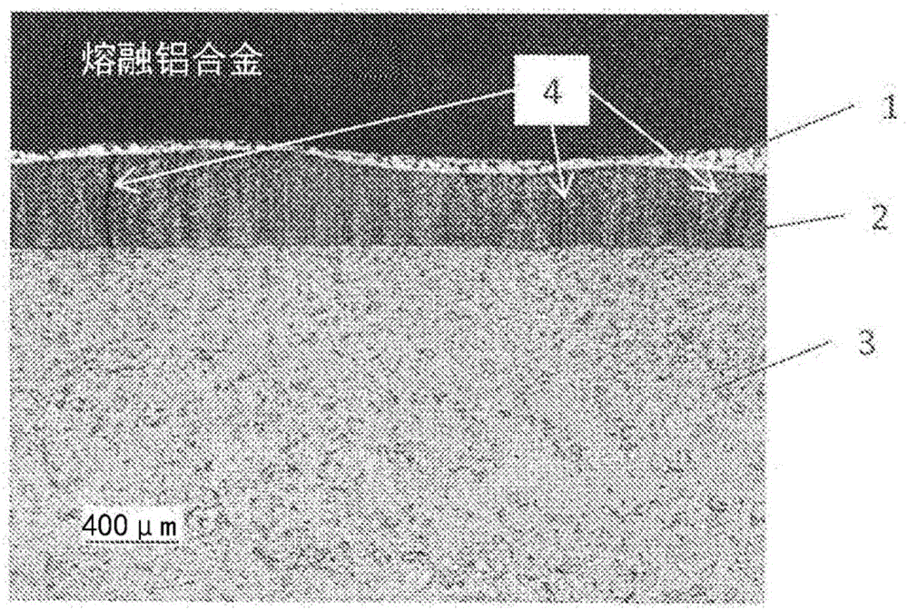
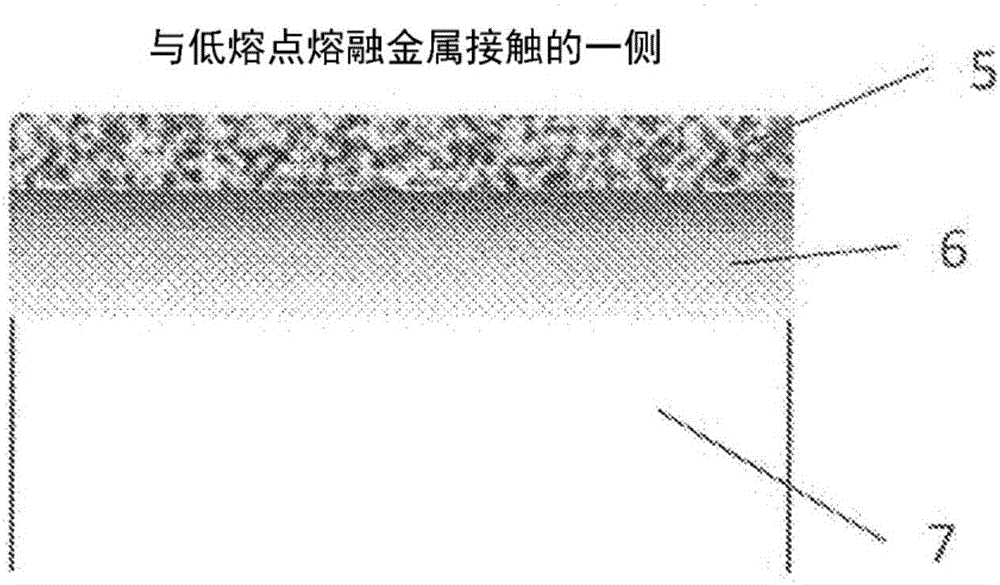
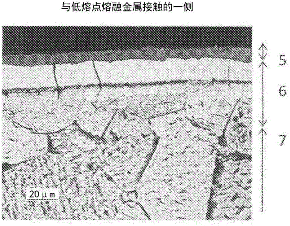
[0109] The surface section of the test piece subjected to the exposure test B was embedded in a resin observation table, polished and etched to prepare an observation sample. The length of about 10 mm of the observation sample was observed with an optical microscope, and the thickness (maximum) of the reaction layer formed by the reaction with "solder" and the presence or absence of cracks were evaluated in order to grasp the degree of erosion resistance.
[0110] In Invention Example Nos. 102, 105, and 1...
PUM
| Property | Measurement | Unit |
|---|---|---|
| thickness | aaaaa | aaaaa |
| thickness | aaaaa | aaaaa |
| thickness | aaaaa | aaaaa |
Abstract
Description
Claims
Application Information
 - Generate Ideas
- Intellectual Property
- Life Sciences
- Materials
- Tech Scout
- Unparalleled Data Quality
- Higher Quality Content
- 60% Fewer Hallucinations
Browse by: Latest US Patents, China's latest patents, Technical Efficacy Thesaurus, Application Domain, Technology Topic, Popular Technical Reports.
© 2025 PatSnap. All rights reserved.Legal|Privacy policy|Modern Slavery Act Transparency Statement|Sitemap|About US| Contact US: help@patsnap.com


