
Diode laser with built-in grating

A laser and semiconductor technology, applied in the field of lasers, can solve the problems of large temperature drift coefficient, power consumption and volume, and achieve the effect of optimizing efficiency, improving working life and high reliability

Active Publication Date: 2019-04-16
THE 44TH INST OF CHINA ELECTRONICS TECH GROUP CORP
View PDF4 Cites 0 Cited by
  • Summary
  • Abstract
  • Description
  • Claims
  • Application Information

AI Technical Summary

Problems solved by technology

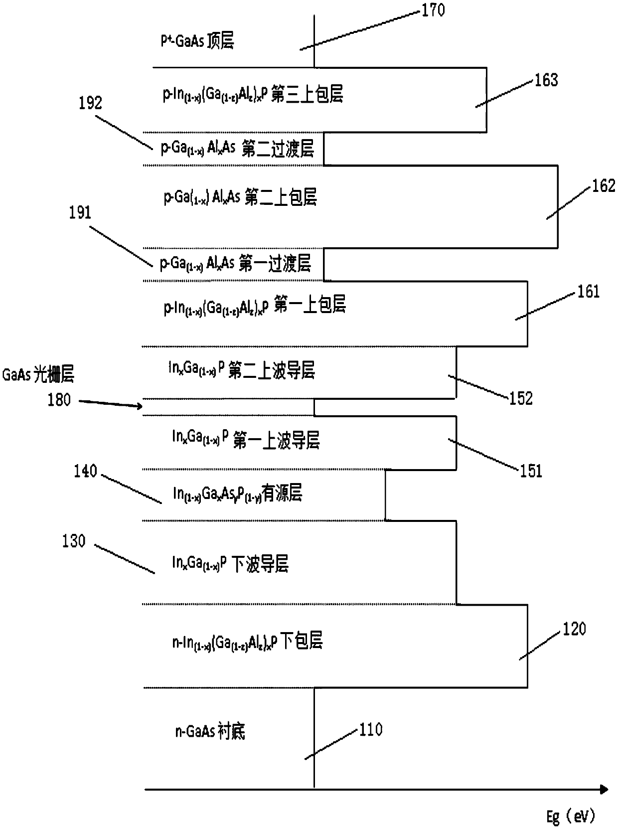
[0004] The invention provides a semiconductor laser with a built-in grating to solve the problem that the current laser pump source wavelength has a large drift coefficient with temperature, and the power consumption and volume caused by it are large

Method used


Image

  • Diode laser with built-in grating
  • Diode laser with built-in grating
  • Diode laser with built-in grating

Examples


Embodiment Construction

[0031] In order to enable those skilled in the art to better understand the technical solutions in the embodiments of the present invention, and to make the above-mentioned purposes, features and advantages of the embodiments of the present invention more obvious and understandable, the following describes the technical solutions in the embodiments of the present invention in conjunction with the accompanying drawings For further detailed explanation.

[0032] In the description of the present invention, unless otherwise specified and limited, it should be noted that the term "connection" should be understood in a broad sense, for example, it can be a mechanical connection or an electrical connection, or it can be the internal communication of two elements, it can be Directly connected or indirectly connected through an intermediary, those skilled in the art can understand the specific meanings of the above terms according to specific situations.

[0033] see figure 1 , is a ...


PUM


Abstract

The invention provides a semiconductor laser with internal optical grating. The semiconductor laser comprises a substrate, a lower covering layer, a lower waveguide layer, an active layer, an upper waveguide layer, an upper covering layer and a top layer sequentially from bottom to top. The upper waveguide layer comprises a first upper waveguide layer and a second upper waveguide layer, the first upper waveguide layer is positioned above the active layer adjacently, the second upper waveguide layer is positioned below the upper covering layer adjacently, and a optical grating layer is arranged between the first upper waveguide layer and the second upper waveguide layer. By the optical grating layer between the first upper waveguide layer and the second upper waveguide layer, spectrum quality and temperature stability of the semiconductor laser can be greatly improved, and power consumption and size of the laser can be reduced.

Description

technical field [0001] The invention belongs to the field of lasers, in particular to a semiconductor laser with a built-in grating. Background technique [0002] With the gradual increase of output optical power, the application of 808nm high-power semiconductor lasers in industrial processing fields such as laser cutting, laser welding and laser cladding modification is expanding day by day. In terms of application methods, the application of semiconductor lasers in industrial processing is divided into two categories: the first category is to directly apply the laser output from the semiconductor laser to the processed material. In order to obtain high output power, an array strip structure, column The array structure of stacked arrays or the beam shaping structure of multiple linear arrays; the second type is to use the semiconductor laser as the pump source of the solid-state laser, so as to solve the problem of the inherent poor spectral characteristics and far-field c...

Claims


Application Information

Patent Timeline
Patent Type & Authority Patents(China)
IPC IPC(8): H01S5/12H01S5/343H01S5/22
CPCH01S5/1237H01S5/2206H01S5/343
Inventor 廖柯
Owner THE 44TH INST OF CHINA ELECTRONICS TECH GROUP CORP
Learn More