Laser holography-based method for processing graphene metal composite surface Raman-enhanced base
A surface Raman enhancement, metal composite technology, applied in optics, optical components, instruments, etc., can solve the problems of high equipment cost, difficult control, long production time, etc., to achieve simple production process, easy accurate control, easy to batch. production effect
- Summary
- Abstract
- Description
- Claims
- Application Information
AI Technical Summary
Problems solved by technology
Method used
Image
Examples
Embodiment 1
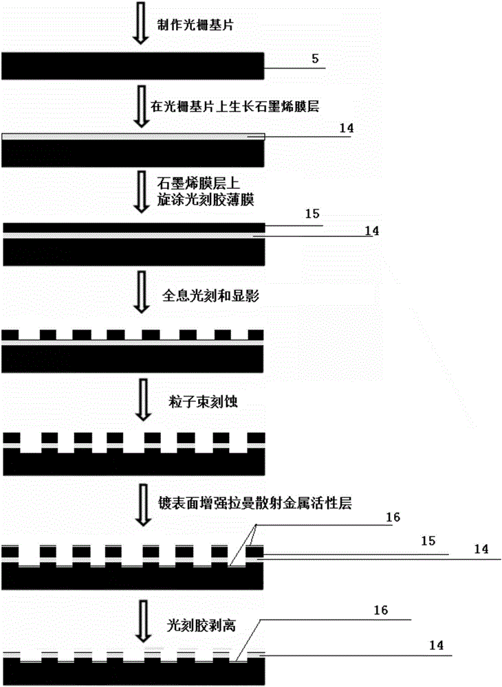
[0035] Embodiment 1: A kind of Raman-enhanced substrate processing method based on laser holographic graphene metal composite surface, such as figure 1 As shown, including the following production steps:
[0036] 1) The step of growing a graphene film layer on the grating substrate 5; using the method of chemical vapor deposition, by optimizing the growth conditions, growing a graphene layer 14 with a thickness of 5 nm to 20 nm on the surface of the clean glass-ceramic grating substrate;
[0037] 2) Spin-coat photoresist film: Clean the grating substrate with a dust-free cloth and organic solvent, start the vacuum equipment of the coater to vacuum before coating, control the rotation speed of the coater, and the photoresist film 15 coating thickness 500nm ~ 600nm;
[0038] Baking hardening film: Put the grating substrate coated with photoresist film into a clean oven at room temperature, heat it quickly and steadily to about 90°C, stay at this temperature for 1 hour, and fina...
Embodiment 2
[0044] Embodiment 2: A kind of Raman-enhanced substrate processing method based on laser holographic graphene metal composite surface, such as figure 1 As shown, including the following production steps:
[0045] 1) The step of growing a graphene film layer on the grating substrate 5; using the method of chemical vapor deposition, by optimizing the growth conditions, growing a graphene layer 14 with a thickness of 10nm on the surface of the clean glass-ceramic grating substrate;
[0046] 2) Spin-coat photoresist film: Clean the grating substrate with a dust-free cloth and organic solvent, start the vacuum equipment of the coater to vacuum before coating, control the rotation speed of the coater, and the photoresist film 15 coating thickness 550nm;
[0047] Baking hardening film: Put the grating substrate coated with photoresist film into a clean oven at room temperature, heat it quickly and steadily to about 90°C, stay at this temperature for 1 hour, and finally lower the ove...
PUM
| Property | Measurement | Unit |
|---|---|---|
| thickness | aaaaa | aaaaa |
| thickness | aaaaa | aaaaa |
| thickness | aaaaa | aaaaa |
Abstract
Description
Claims
Application Information
 - R&D Engineer
- R&D Manager
- IP Professional
- Industry Leading Data Capabilities
- Powerful AI technology
- Patent DNA Extraction
Browse by: Latest US Patents, China's latest patents, Technical Efficacy Thesaurus, Application Domain, Technology Topic, Popular Technical Reports.
© 2024 PatSnap. All rights reserved.Legal|Privacy policy|Modern Slavery Act Transparency Statement|Sitemap|About US| Contact US: help@patsnap.com


