Solution processing preparation method of crystalline Sb2S3 thin film
A solution processing and crystallinity technology, applied in chemical instruments and methods, inorganic chemistry, coatings, etc., can solve the problems of unfavorable large-area preparation, high energy consumption, complex equipment and preparation process, etc. The effect of large particle size and large light absorption coefficient
- Summary
- Abstract
- Description
- Claims
- Application Information
AI Technical Summary
Problems solved by technology
Method used
Image
Examples
Embodiment 1
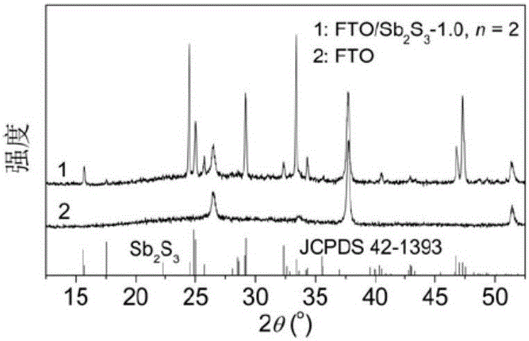
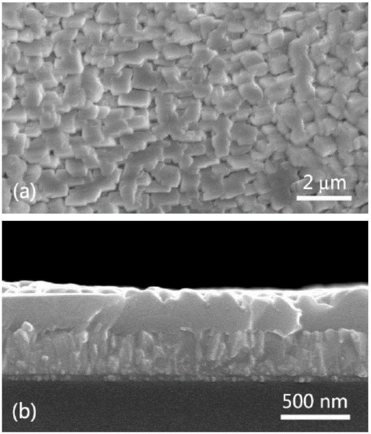
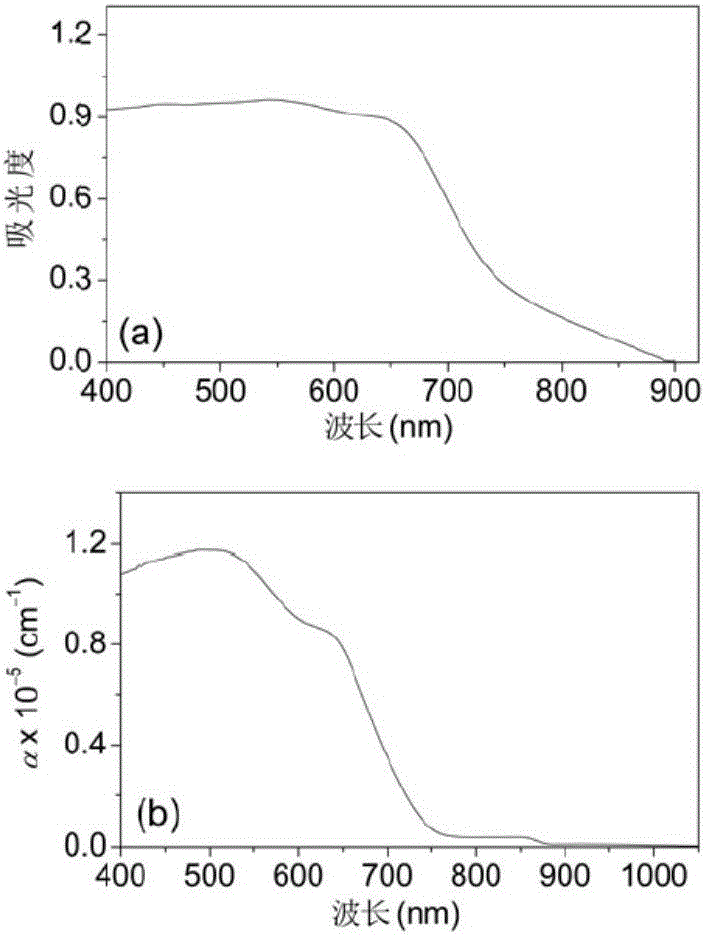
[0032] Embodiment 1: Crystalline Sb on the FTO conductive glass substrate 2 S 3 Film preparation
[0033] (1) Cleaning of FTO conductive glass:
[0034] The FTO conductive glass was ultrasonically cleaned by acetone, isopropanol, and ultrapure water for 5 minutes to obtain a clean FTO conductive glass substrate, which was dried and used for later use.
[0035] (2) SbCl 3 Sb with a concentration of 1.0mol / L 2 S 3 Preparation of reaction precursor solution:
[0036] SbCl at room temperature 3 Dissolve in N,N-dimethylformamide and stir for 0.5 hours to obtain clear SbCl with a concentration of 1.0mol / L 3 solution; then, in the resulting SbCl 3 Add thiourea to the solution, where SbCl 3 The molar ratio to thiourea was 1:1.8, and stirred at room temperature for 0.5 hours to obtain clear SbCl 3 and thiourea mixture solution; finally, add glycerol to this mixture solution, wherein the volume ratio of N,N-dimethylformamide and glycerol is 2.5:1, and stir for 10 minutes to ob...
Embodiment 2
[0041] Example 2: TiO 2 Crystalline Sb on Thin Film Substrate 2 S 3 Film preparation
[0042] (1) cleaning of FTO conductive glass: with embodiment 1.
[0043] (2)TiO 2 Preparation of film backing:
[0044] Mix absolute ethanol, n-butyl titanate, and glacial acetic acid at a volume ratio of 20:5:0.5 to prepare uniform, colorless and transparent TiO 2 Sol precursor. Then, the TiO 2 The sol precursor solution was spin-coated on a clean FTO conductive glass (2500 rpm, 30 seconds) to obtain TiO 2 Sol film; the TiO 2 After the sol film was stored at room temperature in a humidifier with a relative humidity of 50% for 12 hours, it was placed in a muffle furnace in an air atmosphere, and the temperature of the muffle furnace was raised to 550 °C at a heating rate of 1 °C / min. ℃, and kept at this temperature for 30 minutes for TiO 2 Sintering of the sol film; after sintering, let the muffle furnace cool down to room temperature at a rate of 1°C / min to obtain TiO 2 Film subs...
Embodiment 3
[0051] Example 3: TiO 2 Crystalline Sb on Thin Film Substrate 2 S 3 Film preparation
[0052] (1) cleaning of FTO conductive glass: with embodiment 1.
[0053] (2)TiO 2 The preparation of film backing base: with embodiment 2.
[0054] (3) SbCl 3 Sb with a concentration of 1.5mol / L 2 S 3 Preparation of reaction precursor solution:
[0055] SbCl at room temperature 3 Dissolve in N,N-dimethylformamide and stir for 0.5 hours to obtain clear SbCl with a concentration of 1.5mol / L 3 solution; then, in the resulting SbCl 3 Add thiourea to the solution, where SbCl 3 The molar ratio to thiourea was 1:1.8, and stirred at room temperature for 0.5 hours to obtain clear SbCl 3 and thiourea mixture solution; finally, add glycerol to this mixture solution, wherein the volume ratio of N,N-dimethylformamide and glycerol is 2.5:1, and stir for 10 minutes to obtain SbCl 3 Sb with a concentration of 1.5mol / L 2 S 3 Reaction precursor solution. The Sb 2 S 3 The reaction precursor s...
PUM
| Property | Measurement | Unit |
|---|---|---|
| Thickness | aaaaa | aaaaa |
| Thickness | aaaaa | aaaaa |
| Diameter | aaaaa | aaaaa |
Abstract
Description
Claims
Application Information
 - R&D
- Intellectual Property
- Life Sciences
- Materials
- Tech Scout
- Unparalleled Data Quality
- Higher Quality Content
- 60% Fewer Hallucinations
Browse by: Latest US Patents, China's latest patents, Technical Efficacy Thesaurus, Application Domain, Technology Topic, Popular Technical Reports.
© 2025 PatSnap. All rights reserved.Legal|Privacy policy|Modern Slavery Act Transparency Statement|Sitemap|About US| Contact US: help@patsnap.com


