A method of manufacturing vertical LED chips to realize the reuse of sapphire substrates

A sapphire substrate and LED chip technology, applied in semiconductor/solid-state device manufacturing, semiconductor devices, electrical components, etc., can solve problems such as waste, GaN film damage, sapphire substrate surface damage, etc., to improve luminous efficiency and reduce costs Effect

Active Publication Date: 2018-12-07
HEBEI UNIV OF TECH
View PDF6 Cites 0 Cited by
  • Summary
  • Abstract
  • Description
  • Claims
  • Application Information

AI Technical Summary

Problems solved by technology

CN102610578A A matrix type sapphire substrate and a preparation method thereof, the method uses a double-polished sapphire substrate, prepares a matrix on the C surface of the substrate, and then grows epitaxy to improve the growth quality of the GaN epitaxial layer. The double-polished sapphire The substrate is easy to lift off by laser, but the local high temperature generated during the stripping will cause damage to the surface of the sapphire substrate, which is not conducive to reuse, and the GaN film will be damaged due to the rapid release of stress during the stripping; the laser stripping sapphire substrate technology is adopted in the industry, and The sapphire substrate will be ground and thinned before peeling off, and the peeled sapphire substrate can only be treated as waste, resulting in great waste

Method used


Image

  • A method of manufacturing vertical LED chips to realize the reuse of sapphire substrates
  • A method of manufacturing vertical LED chips to realize the reuse of sapphire substrates
  • A method of manufacturing vertical LED chips to realize the reuse of sapphire substrates

Examples


Embodiment 1

[0050] The method for preparing a vertical LED chip of this embodiment includes the following steps:

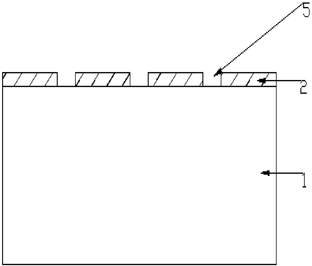
[0051] The first step is to deposit Si on the sapphire substrate by plasma enhanced chemical vapor deposition (PECVD, Plasma Enhanced Chemical Vapor Deposition) 3 N 4 Sacrificial layer (among them, PECVD radio frequency power 60W, substrate temperature 300℃, cavity pressure 500mTorr, SiH 4 Flow 30sccm, NH 3 Flow rate 120sccm, deposition time 160s), sacrificial layer thickness 100nm;

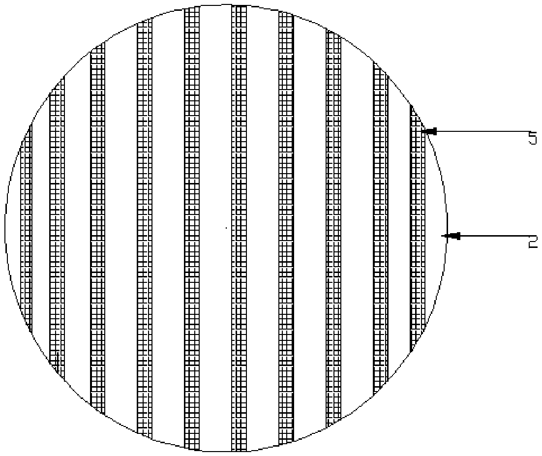
[0052] In the second step, the sacrificial layer is coated, exposed, and developed to prepare a groove pattern, and then a line-shaped groove is prepared by a wet etching method. The groove width is 5μm, the line-to-line spacing is 1mm, and the line-shaped groove The depth is equal to the thickness of the deposited sacrificial layer (that is, the sapphire substrate is exposed at the trench);

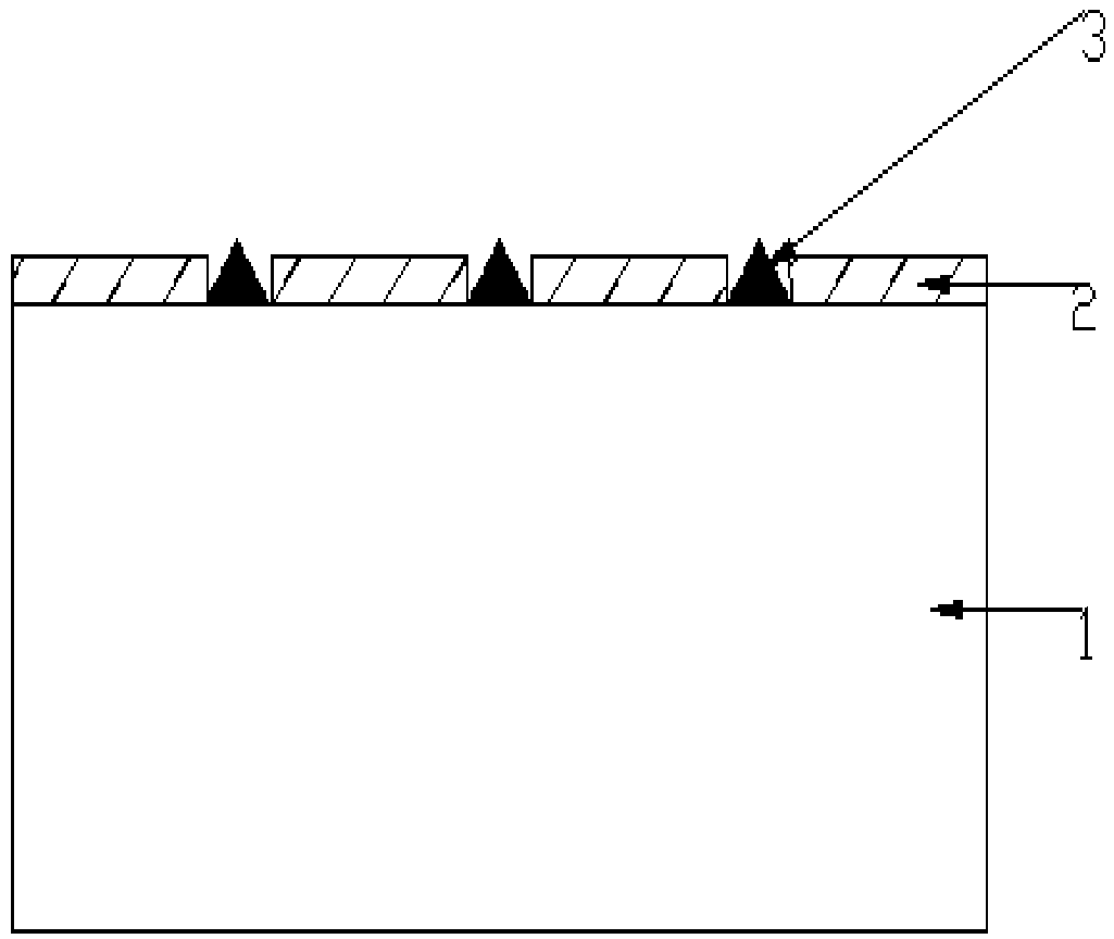
[0053] The third step is to use the Metal-organic Chemical Vapor Deposition (MOCVD) method. Firstly, the GaN b...

Embodiment 2

[0064] The method for preparing a vertical LED chip of this embodiment includes the following steps:

[0065] Except for the first step, Si is prepared on the sapphire substrate by plasma enhanced chemical vapor deposition (PECVD, PlasmaEnhanced Chemical Vapor Deposition). 3 N 4 Sacrificial layer, power 40W, substrate temperature 300℃, working pressure 500mTorr, SiH 4 Flow 30sccm, NH 3 The flow rate is 120sccm, the deposition time is 110s; the thickness of the sacrificial layer is 50nm; in the second step, the sacrificial layer is coated, exposed, and developed to prepare a groove pattern, and then a line-shaped groove is prepared by a wet etching method. The groove width is 3μm, the line-to-line spacing is 0.5mm, and the line-shaped groove depth is equal to the thickness of the deposited sacrificial layer; the third step is to use MOCVD to grow a GaN buffer layer in the groove revealing the sapphire substrate, and then On the basis of the GaN buffer layer, an undoped GaN layer is...

Embodiment 3

[0067] The method for preparing a vertical LED chip of this embodiment includes the following steps:

[0068] Except for the first step, Si is prepared on the sapphire substrate by plasma enhanced chemical vapor deposition (PECVD, PlasmaEnhanced Chemical Vapor Deposition). 3 N 4 Sacrificial layer, power 20W, substrate temperature 300℃, working pressure 500mTorr, SiH 4 Flow 30sccm, NH 3 The flow rate is 120sccm, the deposition time is 390s; the thickness of the sacrificial layer is 80nm; the second step, the sacrificial layer is coated, exposed, and developed to prepare a groove pattern, and then the Si in the groove is removed by wet etching 3 N 4 The sacrificial layer is completely removed, the trench width is 10μm, the line-to-line spacing is 3mm, and the line-shaped trench depth is equal to the thickness of the deposited sacrificial layer; the third step is to grow a GaN buffer in the trench that exposes the sapphire substrate by MOCVD Then, based on the GaN buffer layer, an und...


PUM


Abstract

The invention provides a vertical LED (light-emitting diode) chip preparation method capable of realizing the repeated utilization of a sapphire substrate. According to the method, a sacrificial layer with a strip-shaped trench is prepared on a sapphire substrate with a single polished surface; a GaN buffer layer grows at the bottom of the trench to expose the sapphire substrate; an un-doped GaN layer transversely grows on the surface of the sacrificial layer with a buffer layer inside the trench as a basis; an N-type GaN layer, a quantum well layer and a P-type GaN layer sequentially grow on the surface of the un-doped GaN layer; and metal reflecting layer and a metal bonding layer are prepared on the surface of the P-type GaN layer. The metal bonding layer is prepared on a silicon wafer substrate, and then the metal bonding layer and the silicon wafer substrate are bonded together. After the bonding process, the sacrificial layer is corroded by the HF solution, so that the sapphire substrate with the single polished surface is removed. Finally, the sapphire substrate is subjected to CMP (chemical mechanical polishing) treatment, so that the repeated utilization of the sapphire substrate is realized. Based on the above method, the repeated utilization of the substrate for preparing vertical LED chips is realized, and the production cost is saved.

Description

Technical field [0001] The technical scheme of the present invention relates to a method for preparing a vertical LED chip suitable for reusing a sapphire substrate, and belongs to the field of optoelectronics. Background technique [0002] Traditional LED chips use sapphire as a substrate to grow a GaN epitaxial layer. The sapphire substrate has poor thermal conductivity, which greatly restricts the heat dissipation of the LED. At the same time, its basically non-conductive nature leads to the need to sacrifice part of the light-emitting layer when preparing the N electrode, which has a great impact on the brightness of the LED. [0003] As people’s requirements for LED integration and luminous brightness increase, traditional LED chips can no longer meet the requirements. Therefore, substrate transfer technology is used to replace sapphire with vertical LEDs with good conductivity and high thermal conductivity such as Cu and Si substrates. Chips are currently the focus of resear...

Claims


Application Information

Patent Timeline
Patent Type & Authority Patents(China)
IPC IPC(8): H01L33/20H01L33/00H01L21/86
CPCH01L21/86H01L33/005H01L33/20
Inventor 周朝旭张保国潘柏臣
Owner HEBEI UNIV OF TECH
Why Eureka
Try Eureka