Process for manufacturing power semiconductor module chip with high reliability and high power

A power semiconductor and manufacturing process technology, which is applied in the manufacturing process of high-reliability and high-voltage power semiconductor module chips, can solve problems such as high requirements for curing conditions, poor adhesion and stress, and easy deliquescence of PI glue, so as to improve the recognition degree and anti-counterfeiting ability, high cost performance, and the effect of preventing electron migration

Pending Publication Date: 2016-12-21
HUANGSHAN 777 ELECTRONICS CO LTD
View PDF0 Cites 4 Cited by
  • Summary
  • Abstract
  • Description
  • Claims
  • Application Information

AI Technical Summary

Problems solved by technology

However, commercially available PI adhesives have problems such as deliquescence, bubbles, high curing conditions, poor adhesion and stress, etc.

Method used


Image

  • Process for manufacturing power semiconductor module chip with high reliability and high power
  • Process for manufacturing power semiconductor module chip with high reliability and high power
  • Process for manufacturing power semiconductor module chip with high reliability and high power

Examples


Embodiment Construction

[0022] The description of the present invention is only a preferred embodiment of the invention, and is not intended to limit the invention. Any modification, equivalent replacement and improvement made within the spirit and principle of the invention should be included in the Within the scope of protection of the present invention.

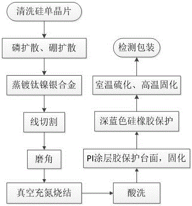
[0023] The present invention proposes a manufacturing process for a high-reliability high-voltage power semiconductor module chip, and the process flow chart is as follows figure 1 shown, including the following steps:

[0024] Step 1. After cleaning the silicon single wafer, perform phosphorus diffusion and boron diffusion, and then vapor-deposit a titanium-nickel-silver alloy layer on both sides of the silicon chip to effectively reduce the forward voltage drop V of the chip. FM , thermal resistance and stress;

[0025] Step 2. Wire-cut the silicon wafer that has completed the diffusion process, and cut it into regular circular units with a d...


PUM

PropertyMeasurementUnit
thicknessaaaaaaaaaa
dielectric lossaaaaaaaaaa

Abstract

The invention relates to a process for manufacturing a power semiconductor module chip with high reliability and high power. The entre manufacturing process comprises the following procedures: phosphorus diffusion, boron diffusion, titanium nickel silver alloy evaporation, linear cutting, angle grinding, vacuum sintering, acid etching, double-layer colloid joint protection, room temperature vulcanization, high temperature curing, detection and package. The double-layer colloid joint protection, as shown in the figure, comprises: uniformly a coating polyimide (PI) adhesive (41 in the figure) on the table top of the chip to form a dense protective layer, and then using a self-developed automatic gumming tool fixture to coat deep blue silicone rubber (42 in the figure) in batches. According to the process provided by the invention, the advantages of GPP square chips and OJ wafers are combined to improve the manufacturing process of the existing power semiconductor module chip so as to effectively prevent electron transfer and reduce high and normal temperature current leakage of the chip, the dense structure is conducive to subsequent module encapsulation and storage to effectively improve the reliability and yield of products.

Description

technical field [0001] The invention belongs to the technical field of semiconductor components, and in particular relates to a manufacturing process of a high-reliability high-voltage power semiconductor module chip. Background technique [0002] In recent years, domestic power semiconductor modules are developing in the direction of high reliability, high performance, multi-combination, high voltage and high frequency, and high cost performance, and are gradually replacing imports. Therefore, the performance requirements for the module chip structure and protective materials are getting higher and higher. In the current production process of silicon rectifier chip OJ (Open Junction) with single corner + white silicone rubber protection, the single-layer silicon rubber chip is susceptible to moisture and has poor mechanical strength. Not only the volt-ampere characteristics of the chip are easily affected, but also creep often occurs; In addition, the colloidal temperature...

Claims


Application Information

Patent Timeline
Patent Type & Authority Applications(China)
IPC IPC(8): H01L21/56H01L21/02H01L29/06H01L29/40
CPCH01L29/0657H01L29/40H01L21/02H01L21/561
Inventor 戴立新冯立康洪国东鲍婕陈珍海
Owner HUANGSHAN 777 ELECTRONICS CO LTD
Why Eureka
Try Eureka