Method for filling organic polymers in conductive or semiconducting micropores
A technology for filling polymers and semiconductors, which is applied in semiconductor/solid-state device manufacturing, electrical components, circuits, etc., can solve problems such as chip short circuits, achieve the effects of buffering stress corrosion resistance, low cost, and improving corrosion resistance
- Summary
- Abstract
- Description
- Claims
- Application Information
AI Technical Summary
Problems solved by technology
Method used
Image

Examples
Embodiment 1
[0025] This embodiment relates to a method for filling organic polymers in conductor or semiconductor micropores, the specific steps are as follows:
[0026] Step (1): Put the copper sheet with micropores on the surface into acetone and ethanol for degreasing treatment, then pickle to remove oxides on the surface of the substrate, and finally rinse the surface of the substrate with pure water;
[0027] Step (2): Put the cleaned copper sheet into the configured aqueous phase solution, its components are 0.01g / mL sodium dodecylsulfonate, 6% volume fraction of acrylic acid, 0.002g / mL of Diazonium tetrafluoroborate, 0.01g / mL EDTA-2Na;
[0028] Step (3): Take out the sample after reacting for a period of time, and measure the thickness of the organic matter at the section;
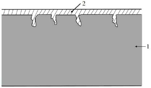
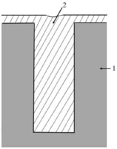
[0029] Step (4): Adjust the reaction time according to the thickness in step (3), and repeat steps (1) to (3), so that the organic matter deposited on the copper substrate can fill the defects in the pores; th...
Embodiment 2
[0031] This embodiment relates to a method for filling organic polymers in conductor or semiconductor micropores, the specific steps are as follows:
[0032] Step (1): Put the p-type silicon chip with a resistivity of 5Ω·cm and micropores into acetone and ethanol for degreasing treatment, then pickle to remove oxides on the surface of the substrate, and finally clean the substrate with pure water Rinse the surface clean;
[0033] Step (2): Put the cleaned silicon chip into the configured aqueous phase solution, its components are 0.01g / mL sodium dodecylsulfonate, 6% volume fraction of acrylic acid, 0.002g / mL of Pyrazole diazonium inner salt, 0.01g / mL of EDTA-2Na;
[0034] Step (3): Take out the sample after reacting for a period of time, and measure the thickness of the organic matter at the section;
[0035] Step (4): adjusting the reaction time according to the thickness in step (3), and repeating steps (1) to (3), so that the organic matter deposited on the silicon wafer ...
Embodiment 3
[0037] This embodiment relates to a method for filling organic polymers in conductor or semiconductor micropores, the specific steps are as follows:
[0038] Step (1): Put the n-type GaAs sheet with a resistivity of 50Ω·cm and micropores into acetone and ethanol for degreasing treatment, then pickle to remove oxides on the surface of the substrate, and finally wash the substrate with pure water Rinse the surface clean;
[0039] Step (2): Put the cleaned GaAs sheet into the prepared aqueous phase solution, the components of which are 1g / mL sodium dodecylsulfonate, 6% volume fraction of acrylic acid, 0.002g / mL tris Pterene diazonium salt, 0.01g / mL EDTA-2Na;
[0040] Step (3): Take out the sample after reacting for a period of time, and measure the thickness of the organic matter at the section;
[0041] Step (4): Adjust the reaction time according to the thickness in step (3), and repeat steps (1) to (3), so that the organic matter deposited on the GaAs sheet can fill the defe...
PUM
| Property | Measurement | Unit |
|---|---|---|
| electrical resistivity | aaaaa | aaaaa |
Abstract
Description
Claims
Application Information
 - Generate Ideas
- Intellectual Property
- Life Sciences
- Materials
- Tech Scout
- Unparalleled Data Quality
- Higher Quality Content
- 60% Fewer Hallucinations
Browse by: Latest US Patents, China's latest patents, Technical Efficacy Thesaurus, Application Domain, Technology Topic, Popular Technical Reports.
© 2025 PatSnap. All rights reserved.Legal|Privacy policy|Modern Slavery Act Transparency Statement|Sitemap|About US| Contact US: help@patsnap.com