High thermal stability superjunction strained si/sige heterojunction bipolar transistor
A heterojunction bipolar, high thermal stability technology, applied in semiconductor devices, electrical components, circuits, etc., can solve problems such as exacerbating thermal instability, limiting high-power stable operation of devices, and drifting of static operating points to achieve sensitive Effects of performance improvement, large current gain, and high breakdown voltage characteristics
- Summary
- Abstract
- Description
- Claims
- Application Information
AI Technical Summary
Problems solved by technology
Method used
Image
Examples
Embodiment 1
[0026] figure 1 shows the longitudinal cross-sectional structure of a strained Si / SiGe heterojunction bipolar transistor with a superjunction p-type layer, including sequentially epitaxially grown n + Doped SiGe dummy substrate (10), whose Ge content gradually changes from 0 to 0.15; n + doped relaxed Si 1-y Ge y Sub-collector (11), its Ge composition y=0.15; n - doped relaxed Si 1-y Ge y Collector region (12), its Ge composition y=0.15; superjunction p-type layer (13), intrinsically strained Si 1-x Ge x Lower buffer layer (14); p + doped strained Si 1-x Ge x Base region (15), its Ge component content x=0.3; intrinsically strained Si 1-x Ge x Upper buffer layer (16); p + Doped SiGe extrinsic base region (17); n-doped strained Si emitter region (18); silicon dioxide (SiO 2 ) layer (19) and metal leads (20).
[0027] The super junction p-type layer (13) is located on the relaxed Si 1-y Ge y In the collector region (12), parallel to the strained Si 1-x Ge x The ...
Embodiment 2
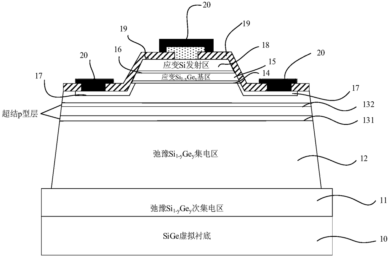
[0032] image 3 shows the longitudinal cross-sectional structure of a strained Si / SiGe heterojunction bipolar transistor with two superjunction p-type layers, including sequentially epitaxially grown n + Doped SiGe dummy substrate (10), whose Ge content gradually changes from 0 to 0.15; n + doped relaxed Si 1-y Ge y Sub-collector (11), its Ge composition y=0.15; n - doped relaxed Si 1-y Ge y Collector region (12), its Ge composition y=0.15; the lower layer of the two-layer superjunction p-type layer (131); the upper layer of the two-layer superjunction p-type layer (132); intrinsically strained Si 1-x Ge x Lower buffer layer (14); p + doped strained Si 1-x Ge x Base region (15), its Ge component content x=0.3; intrinsically strained Si 1-x Ge x Upper buffer layer (16); p + Doped Si 1-x Ge x Extrinsic base region (17), n-doped strained Si emitter region (18); silicon dioxide (SiO 2 ) layer (19) and metal leads (20).
[0033] The lower layer of the two-layer supe...
PUM
 Abstract
Description
Claims
Application Information
 - R&D
- Intellectual Property
- Life Sciences
- Materials
- Tech Scout
- Unparalleled Data Quality
- Higher Quality Content
- 60% Fewer Hallucinations
Browse by: Latest US Patents, China's latest patents, Technical Efficacy Thesaurus, Application Domain, Technology Topic, Popular Technical Reports.
© 2025 PatSnap. All rights reserved.Legal|Privacy policy|Modern Slavery Act Transparency Statement|Sitemap|About US| Contact US: help@patsnap.com


