Preparation method of stress controllable silicon-based thin film
A silicon-based film and stress technology, which is applied in semiconductor/solid-state device manufacturing, electrical components, circuits, etc., can solve problems such as unobtainable and limited influence of stress, and achieve reduced production cycle, high controllability, and improved material The effect of application range
- Summary
- Abstract
- Description
- Claims
- Application Information
AI Technical Summary
Problems solved by technology
Method used
Image
Examples
Embodiment 1
[0037] Preparation of SiN thin film on substrate material Si:
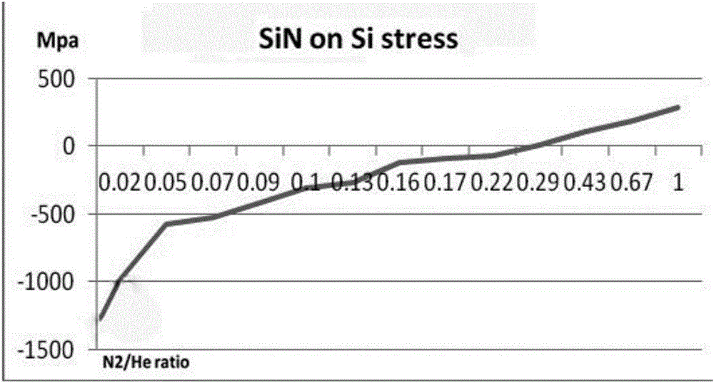
[0038] Use 10wt% HCl deionized aqueous solution to clean the Si substrate and put it into the cavity of a single-frequency PECVD equipment with a frequency of 13.56MHz, and then feed the raw material gas SiH 4 , NH 3 and N 2 , He is evenly introduced into the cavity from the spray hole on the top of the cavity, the temperature in the cavity is set to 250 ° C, the pressure in the cavity is set to 1500 mTorr, the power of the radio frequency source is set to 150 W during the preparation process, and the SiH 4 The flow rate is 400sccm, NH 3 The flow rate is 20sccm, N 2 The flow rate is 0~5000sccm, the He flow rate is 0~5000sccm, the actual flow rate is adjusted according to the flow ratio, the film deposition rate is greater than 20nm / min, the deposition time is 3min, and the N is adjusted from close to 0 2 / He flow ratio to 1, as attached figure 1 N shown 2 / He flow ratio and film stress change trend graph, th...
Embodiment 2
[0042] Preparation of SiN thin films on the substrate material GaAs:
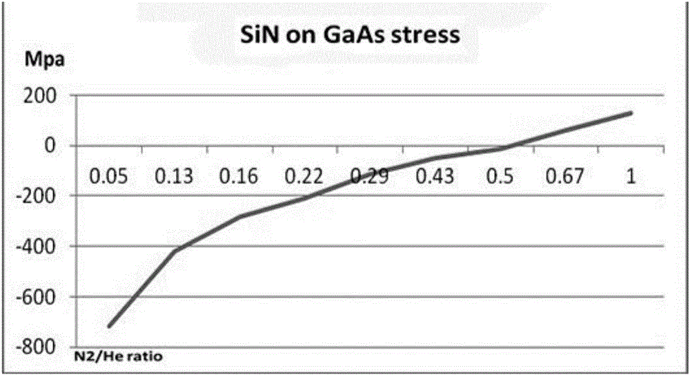
[0043]Use 10wt% HCl deionized aqueous solution to clean the GaAs substrate and put it into the cavity of a single-frequency PECVD equipment with a frequency of 13.56MHz, and then feed the raw material gas SiH 4 , NH 3 and N 2 , He is evenly introduced into the cavity from the spray hole on the top of the cavity, the temperature in the cavity is set to 300°C, the pressure in the cavity is set to 2000mTorr, the power of the radio frequency source is set to 180W during the preparation process, SiH 4 Flow rate is 700sccm, NH 3 The flow rate is 50sccm, N 2 The flow rate is 0~5000sccm, the He flow rate is 0~5000sccm, the film deposition rate is greater than 35nm / min, the deposition time is 5min, and the N is adjusted from close to 0. 2 / He flow ratio to 1, as attached figure 2 N shown 2 / He flow rate ratio and film stress change trend graph (where X-axis is N 2 / He flow ratio, Y-axis is stress) The stress...
Embodiment 3
[0047] Preparation of SiN thin film on substrate material SiC:
[0048] Use 10wt% HCl deionized aqueous solution to clean the SiC substrate and put it into the cavity of a flat-panel single-frequency PECVD equipment with a frequency of 2.45 GHz, and then feed the raw material gas SiH 4 , NH 3 and N 2 , He is evenly introduced into the cavity from the spray hole on the top of the cavity, the temperature in the cavity is set to 350°C, the pressure in the cavity is set to 3000mTorr, the power of the radio frequency source is set to 500W during the preparation process, SiH 4 Flow rate is 700sccm, NH 3 The flow rate is 50sccm, N 2 The flow rate is 0~5000sccm, the He flow rate is 0~5000sccm, the film deposition rate is greater than 30nm / min, the deposition time is 4min, and the N is adjusted from close to 0. 2 / He flow ratio to 10, in the adjustment process, the stress test equipment used to test the stress of different SiN films obtained, the test uses the stress tester of TOHO...
PUM
 Abstract
Description
Claims
Application Information
 - R&D
- Intellectual Property
- Life Sciences
- Materials
- Tech Scout
- Unparalleled Data Quality
- Higher Quality Content
- 60% Fewer Hallucinations
Browse by: Latest US Patents, China's latest patents, Technical Efficacy Thesaurus, Application Domain, Technology Topic, Popular Technical Reports.
© 2025 PatSnap. All rights reserved.Legal|Privacy policy|Modern Slavery Act Transparency Statement|Sitemap|About US| Contact US: help@patsnap.com


