Eureka AIR delivers breakthrough ideas for toughest innovation challenges, trusted by R&D personnel around the world.

Copper block burying method of printed circuit board

A technology of printed circuit boards and buried copper blocks, which is applied in the fields of printed circuit, printed circuit, and printed circuit manufacturing. High pass rate and good binding effect

Active Publication Date: 2016-11-16
KINWONG ELECTRONICS TECH LONGCHUAN
View PDF3 Cites 10 Cited by
  • Summary
  • Abstract
  • Description
  • Claims
  • Application Information

AI Technical Summary

Problems solved by technology

However, the existing manufacturing process has problems such as insufficient bonding force between the copper block and the base material, poor connection effect, overflowing glue, difficult grinding, and low product qualification rate, which seriously limits the development and promotion of printed circuit board buried copper block technology.

Method used


Image

  • Copper block burying method of printed circuit board

Examples


Embodiment Construction

[0029] The present invention will be further described below in conjunction with accompanying drawing and specific embodiment:

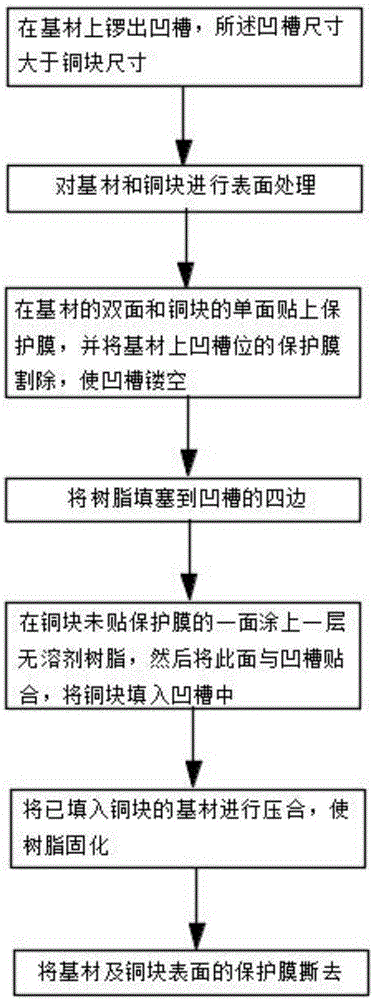
[0030] Such as figure 1 Shown, the printed circuit board buried copper block method of the present invention comprises the following steps:

[0031] (1) Use CNC to control the depth of the base material out of the groove, the size of the groove is larger than the size of the copper block, preferably, the size of the groove is 0.1-0.5mm larger than the size of the copper block;

[0032] (2) Carry out browning treatment to base material and copper block surface;

[0033] (3) affix protective film on both sides of base material and single side of copper block, described protective film is preferably high-temperature protective film, and the protective film of groove position on the base material is cut off, and groove is hollowed out;

[0034] (4) Use dispensing equipment to fill the pre-prepared resin to the four sides of the groove, the filling widt...


PUM


Abstract

The invention relates to the field of production and manufacturing of printed circuit boards, in particular to a copper block burying method of a printed circuit board. The method comprises the following steps: forming a groove in a substrate, wherein the size of the groove is larger than the size of a copper block; carrying out surface treatment on the substrate; adhering a protective film to each of two sides of the substrate and adhering a protective film to one side of the copper block and cutting off the protective film from the groove position on the substrate to hollow the groove; filling the four sides of the groove with resin; smearing a layer of solvent-free resin on the side, without the protective film, of the copper block and adhering the side to the groove; pressing the substrate in which the copper block is buried and curing the resin; and removing the protective films from the surfaces of the substrate and the copper block.

Description

technical field [0001] The invention relates to the field of production and manufacture of printed circuit boards, in particular to a method for embedding copper blocks in printed circuit boards. Background technique [0002] With the rapid development of electronic products in the direction of lightness, thinness, smallness, high density and multi-function, the volume of electronic components and logic circuits has been doubled, while the operating frequency has increased sharply, and the power consumption has continued to increase, resulting in a shift in the working environment of components. The change of high temperature direction puts forward higher and higher requirements for the heat dissipation of PCB products. [0003] Embedding high thermal conductivity metal copper blocks directly in the printed circuit board is one of the effective ways to solve the heat dissipation problem. However, the existing manufacturing process has problems such as insufficient bonding f...

Claims


Application Information

Patent Timeline
Patent Type & Authority Applications(China)
IPC IPC(8): H05K3/00H05K3/38
CPCH05K3/0011H05K3/0044H05K3/381H05K3/382H05K3/386H05K2201/10416
Inventor 陈毅龙谭小林刘火阳巫延俊
Owner KINWONG ELECTRONICS TECH LONGCHUAN
Why Eureka
Eureka Blog
Learn More