Manufacturing method of silicon-based gallium nitride LED epitaxial structure

A silicon-based gallium nitride and manufacturing method technology, applied in ion implantation plating, coating, electrical components, etc., can solve problems such as eliminating the formation of silicon nitride, reduce stress and defect density, improve quality, and improve optoelectronics The effect of conversion efficiency

Active Publication Date: 2016-08-31
FOCUS LIGHTINGS SCI & TECH
View PDF5 Cites 4 Cited by
  • Summary
  • Abstract
  • Description
  • Claims
  • Application Information

AI Technical Summary

Problems solved by technology

[0009] However, neither of the above two technical solutions can fundamentally eliminate the formation of silicon nitride.

Method used


Image

  • Manufacturing method of silicon-based gallium nitride LED epitaxial structure

Examples


Embodiment Construction

[0031] In order to enable those skilled in the art to better understand the technical solutions in the present invention, the technical solutions in the embodiments of the present invention will be clearly and completely described below in conjunction with the drawings in the embodiments of the present invention. Obviously, the described The embodiments are only some of the embodiments of the present invention, not all of them. Based on the embodiments of the present invention, all other embodiments obtained by persons of ordinary skill in the art without making creative efforts shall fall within the protection scope of the present invention.

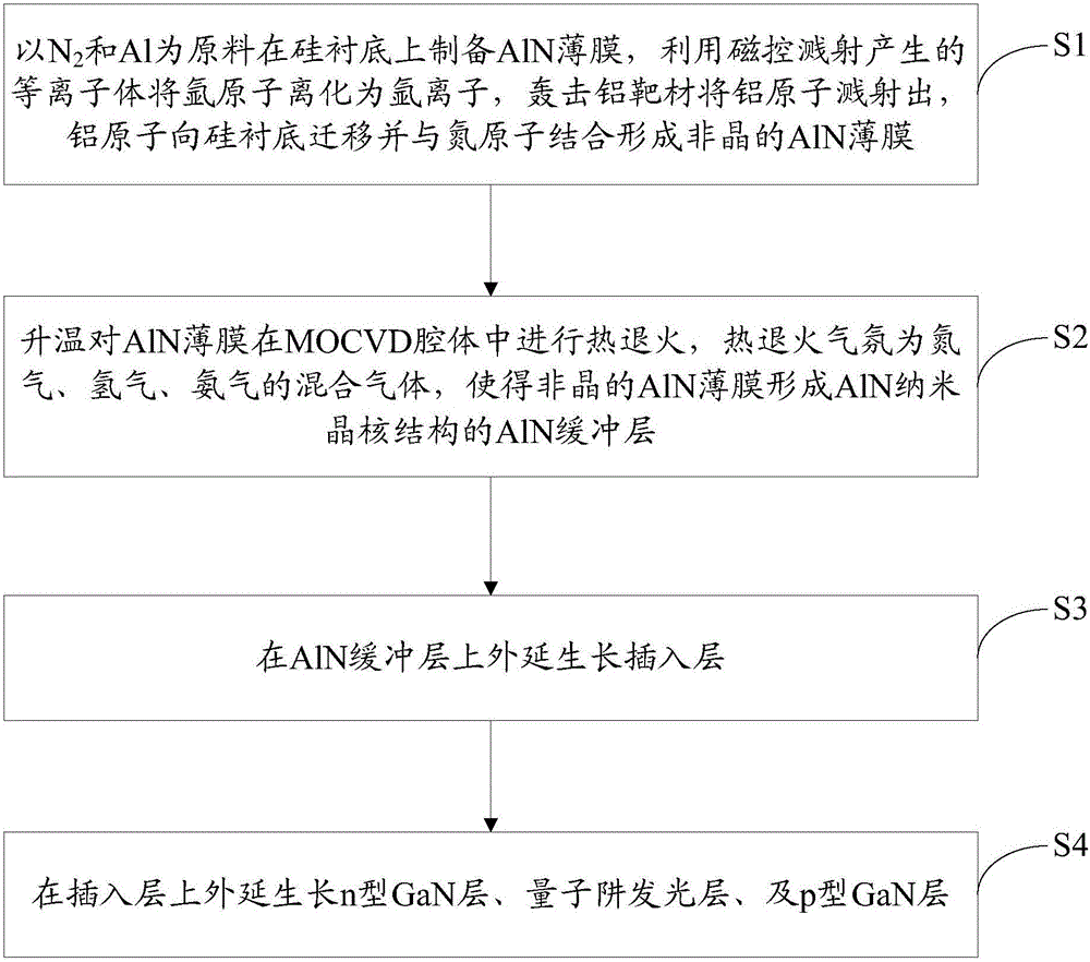
[0032] ginseng figure 1 As shown, the present invention discloses a method for manufacturing an epitaxial structure of a silicon-based gallium nitride LED, which specifically includes:

[0033] S1, with N 2 and Al as raw materials to prepare AlN thin films on silicon substrates, use the plasma generated by magnetron sputtering to ioni...


PUM

PropertyMeasurementUnit
temperatureaaaaaaaaaa
thicknessaaaaaaaaaa

Abstract

The invention provides a manufacturing method of a silicon-based gallium nitride LED epitaxial structure. The manufacturing method comprises the following steps: (S1) with N2 and Al as raw materials, an AlN thin film is prepared on a silicon substrate, argon atoms are ionized into argon ions by plasma generated by magnetron sputtering, an aluminum target material is bombarded to sputter aluminum atoms and the aluminum atoms are migrated towards the silicon substrate and combined with nitrogen atoms to form an amorphous AlN thin film; (S2) the AlN thin film is heated for thermal annealing in an MOCVD cavity, a thermal annealing atmosphere is a mixed gas of nitrogen, hydrogen and an ammonia gas and the amorphous AlN thin film forms an AlN buffer layer of an AlN nano crystal nucleus structure; (S3) an insertion layer is formed on the AlN buffer layer in an epitaxial growth manner; and (S4) an n-type GaN layer, a quantum well light-emitting layer and a p-type GaN layer are formed on the insertion layer in an epitaxial growth manner. By the manufacturing method, the quality of the AlN film deposited by magnetron sputtering is improved; and the stress and the defect density caused by epitaxial film lattice mismatch are reduced.

Description

technical field [0001] The invention relates to the technical field of LEDs, in particular to a method for manufacturing an epitaxial structure of a silicon-based gallium nitride LED. Background technique [0002] A light-emitting diode (Light-Emitting Diode, LED) is a semiconductor electronic component that can emit light. This electronic component appeared as early as 1962. In the early days, it could only emit red light with low luminosity. Later, other monochromatic light versions were developed. Today, the light that can be emitted has covered visible light, infrared rays and ultraviolet rays, and the luminosity has also increased to a considerable extent. of luminosity. And the use is also used as indicator lights, display panels, etc. from the beginning; with the continuous advancement of technology, light-emitting diodes have been widely used in displays, TV lighting decoration and lighting. [0003] Currently commercialized gallium nitride-based semiconductor opto...

Claims


Application Information

Patent Timeline
Patent Type & Authority Applications(China)
IPC IPC(8): H01L33/00H01L33/12C23C14/35C23C14/06C23C14/58
CPCC23C14/0036C23C14/0617C23C14/35C23C14/5806H01L33/007H01L33/12
Inventor 冯猛陈立人刘恒山
Owner FOCUS LIGHTINGS SCI & TECH
Why Eureka
Try Eureka