
Preparation method for novel hafnium-silicon-tantalum-oxygen-nitrogen high-dielectric-constant gate dielectric

A hafnium-silicon-tantalum-oxygen-nitride technology with high dielectric constant, which is applied in the field of semiconductor device preparation, can solve problems such as increased power consumption and increased gate dielectric leakage, and achieve the effect of adjusting the work function of large metal gates

Inactive Publication Date: 2016-08-17
XIAJIN POWER SUPPLY CO STATE GRID SHANDONG ELECTRIC POWER CO
View PDF3 Cites 3 Cited by
  • Summary
  • Abstract
  • Description
  • Claims
  • Application Information

AI Technical Summary

Problems solved by technology

[0004] The present invention can obtain a gate dielectric material with a higher dielectric constant by introducing Ta into the gate dielectric, and solves the problems of a sharp increase in gate dielectric leakage and a serious increase in power consumption as the thickness of the gate dielectric of small-sized devices decreases. , meanwhile, at the interface Ta 2 o 5 The introduction of SiO is beneficial to the adjustment of the metal gate work function of N-type metal oxide semiconductor devices. 2 The introduction of HfON is beneficial to reduce the Ta 2 o 5 The influence of the work function adjustment ability, so that it has a greater metal gate work function adjustment ability

Method used


Image

  • Preparation method for novel hafnium-silicon-tantalum-oxygen-nitrogen high-dielectric-constant gate dielectric

Examples


Embodiment Construction

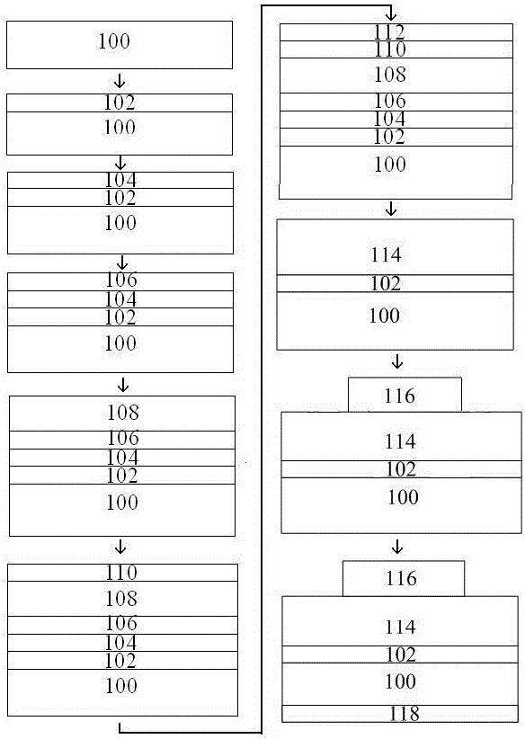
[0007] Through the following description of the embodiments of the present invention with reference to the accompanying drawings, the above and other objects, features and advantages of the present invention will be more clear: figure 1 A cross-sectional view of the gate dielectric structure corresponding to each step in the process of manufacturing the HfSiTaON high dielectric constant gate dielectric according to the embodiment of the present invention is shown. Embodiments of the present invention are described in detail below, examples of which are shown in the drawings, wherein the same or similar reference numerals designate the same or similar elements or elements having the same or similar functions throughout. The embodiments described below by referring to the figures are exemplary only for explaining the present invention and should not be construed as limiting the present invention. A schematic diagram of a layer structure according to an embodiment of the inventio...


PUM

PropertyMeasurementUnit
thicknessaaaaaaaaaa

Abstract

The invention relates to a preparation method for a novel hafnium-silicon-tantalum-oxygen-nitrogen (HfSiTaON) high-dielectric-constant gate dielectric. The preparation method is characterized by comprising the steps of cleaning a silicon wafer, and then oxidizing the cleaned silicon wafer before deposition; depositing a tantalum pentoxide (Ta<2>O<5>), silicon oxide (SiO<2>) and hafnium-oxygen-nitrogen (HfON) laminated gate dielectric on the oxidized silicon wafer, wherein Ta<2>O<5> is positioned on the upper and lower interface of the laminated gate dielectric; SiO<2> is positioned between HfON and Ta<2>O<5>; carrying out ultrasonic washing on the silicon wafer after the laminated gate dielectric is deposited; then carrying out deposition on the cleaned silicon wafer and annealing to form the hafnium-silicon-tantalum-oxygen-nitrogen (HfSiTaON) high-dielectric-constant gate dielectric; forming a metal gate on the annealed silicon wafer; and sputtering aluminum and alloy on the back surface. According to the preparation method, Ta is introduced to the gate dielectric, so that a gate dielectric material with a relatively high dielectric constant can be obtained; the problems of sharp rise of electric leakage and heavily increased power consumption of the gate dielectric caused by decreasing of the thickness of the gate dielectric of small-sized devices are solved; and the prepared gate dielectric has a higher metal gate work function adjustment capability.

Description

technical field [0001] The invention relates to the technical field of semiconductor device preparation, in particular to a method for preparing a hafnium-silicon-tantalum-oxynitride (HfSiTaON) high-permittivity gate dielectric used in the manufacture of nanoscale N-type metal oxide semiconductor devices. Background technique [0002] For more than 40 years, integrated circuit technology has continued to develop according to Moore's law, with the feature size continuously reduced and the integration level continuously improved. As the device size continues to decrease, the thickness of the gate oxide layer decreases accordingly. When the feature size of Metal Oxide Field Effect Transistor (MOSFET) enters 45nm, the gate oxide thickness has been reduced to less than 1.2nm. If the traditional silicon oxide or silicon nitride oxide gate dielectric is still used, the direct tunneling current will increase exponentially. Therefore, in 2007, Intel Corporation began to introduce h...

Claims


Application Information

Patent Timeline
Patent Type & Authority Applications(China)
IPC IPC(8): H01L21/02H01L21/285H01L29/423H01L29/51
CPCH01L29/42364H01L21/02164H01L21/02181H01L21/02183H01L21/022H01L21/02266H01L21/0228H01L21/02301H01L21/02312H01L21/02337H01L29/517H01L29/518
Inventor 滕昭新
Owner XIAJIN POWER SUPPLY CO STATE GRID SHANDONG ELECTRIC POWER CO
Learn More