Composite metal foil, composite metal foil with carrier, metal-clad laminate obtained using said composite metal foil or said composite metal foil with carrier, and printed wiring board
A technology for metal-clad laminates and printed circuit boards, used in printed circuits, printed circuit manufacturing, metal layered products, etc., can solve the problems of micro-cracks, lack of flexibility, etc., and achieve the effect of good signal transmission speed
- Summary
- Abstract
- Description
- Claims
- Application Information
AI Technical Summary
Problems solved by technology
Method used
Image
Examples
Embodiment 1
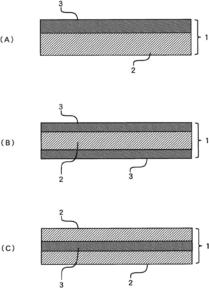
[0073] In embodiment 1, with untreated copper foil (thickness T Cu 12μm electrolytic copper foil), after electroplating the nickel-molybdenum alloy with the thickness shown in Table 1 on both sides (the total thickness of both sides), the obtained figure 1 The layer structure of "nickel-molybdenum alloy layer 3 / copper layer 2 / nickel-molybdenum alloy layer 3" shown in (B), 4 kinds of composite metal foils 1 with equal thickness of the nickel-molybdenum alloy plating layer on both sides (implementation test) Sample 1 to implement sample 4). The nickel-molybdenum alloy plating solution and plating conditions at this time are as follows.
[0074] (nickel-molybdenum alloy plating solution and plating conditions)
[0075] Nickel sulfate hexahydrate: 40g / L
[0076] Sodium molybdate 2 hydrate: 25g / L
[0077] 3 sodium citrate: 80g / L
[0078] Solution pH: 9
[0079] Current density: 16A / dm 2
[0080] Anode electrode: insoluble anode
[0081] Then, the thermal expansion coeffici...
Embodiment 2
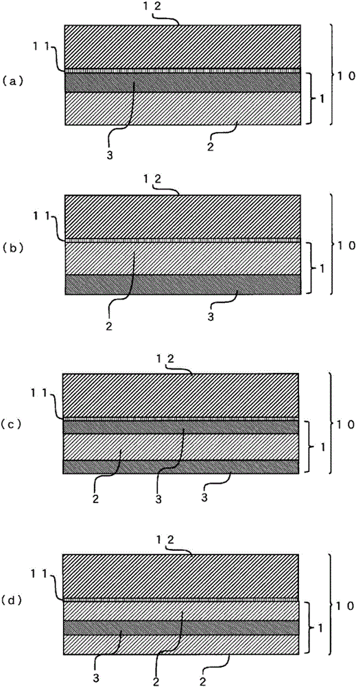
[0105] In embodiment 2, manufactured have figure 2 Composite metal foil with carrier foil with a layer structure of "copper layer 2 / nickel-molybdenum alloy layer 3 / copper layer 2 / peeling layer 11 / carrier 12" shown in (d) (implementation sample 5 to implementation sample 7), and have figure 2 Composite metal foil with carrier foil with a layer structure of "nickel-molybdenum alloy layer 3 / copper layer 2 / nickel-molybdenum alloy layer 3 / peeling layer 11 / carrier 12" shown in (c) (implementation sample 8) . Hereinafter, the manufacturing methods of Example 5 to Example 8 will be described.
[0106] Formation of carrier foils and release layers used in sample 5 to sample 8
[0107] Electrolytic copper foil with a thickness of 18 μm was used as the carrier foil, and on the surface of the carrier foil, the carrier foil was mixed with sulfuric acid 150 g / L, copper concentration 10 g / L, carboxybenzotriazole concentration 800 mg / L, and liquid temperature 30°C. Soak in the dilute su...
PUM
| Property | Measurement | Unit |
|---|---|---|
| Thickness | aaaaa | aaaaa |
| Current density | aaaaa | aaaaa |
| Resistance | aaaaa | aaaaa |
Abstract
Description
Claims
Application Information
 - R&D Engineer
- R&D Manager
- IP Professional
- Industry Leading Data Capabilities
- Powerful AI technology
- Patent DNA Extraction
Browse by: Latest US Patents, China's latest patents, Technical Efficacy Thesaurus, Application Domain, Technology Topic, Popular Technical Reports.
© 2024 PatSnap. All rights reserved.Legal|Privacy policy|Modern Slavery Act Transparency Statement|Sitemap|About US| Contact US: help@patsnap.com


