All-solid-state flexible and stretchable fibrous aluminum air battery and preparation method thereof
A fibrous aluminum and air battery technology, which is applied to battery electrodes, fuel cell half-cells, primary battery-type half-cells, circuits, etc., can solve the problems that cannot meet the requirements of flexibility and stretchability, and achieve large-scale Effects of scale application, weight and volume reduction, prevention of short circuit and electrolyte leakage
- Summary
- Abstract
- Description
- Claims
- Application Information
AI Technical Summary
Problems solved by technology
Method used
Image
Examples
Embodiment 1
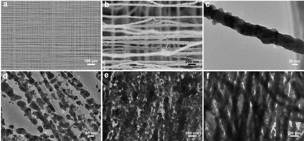
[0022] (1) CNT arrays were prepared by chemical vapor deposition: a catalyst was prepared by depositing a nanometer-thick film on a Si wafer by an electron beam evaporation coating device, and its composition was silicon (Si) / silicon dioxide (SiO 2 ) / alumina (Al 2 o 3 ) / iron (Fe), Al 2 o 3 As a buffer layer between the silicon wafer and Fe, Fe acts as a catalyst. Among them, SiO 2 layer thickness of 400 μm, Al 2 o 3 The layer thickness was 3 nm, and the Fe layer thickness was 1.2 nm. Put the catalyst-coated Si substrate catalyst side up, use a larger silicon wafer as the substrate, and put it into the quartz tube of the tube furnace, near the central part of the tube furnace. Adjust the flow rate of the ventilation pipeline as follows: Argon: 400 sccm; Hydrogen: 30 sccm; Ethylene: 90 sccm. Connect the tubing. First turn on the argon, turn off the hydrogen and ethylene gases. Ventilate at room temperature for 10 minutes to ensure the removal of oxygen and water vapor ...
Embodiment 2
[0027] (1) CNT arrays were prepared by chemical vapor deposition: a catalyst was prepared by depositing a nanometer-thick film on a Si wafer by an electron beam evaporation coating device, and its composition was silicon (Si) / silicon dioxide (SiO 2 ) / alumina (Al 2 o 3 ) / iron (Fe), Al 2 o 3 As a buffer layer between the silicon wafer and Fe, Fe acts as a catalyst. Among them, SiO 2 layer thickness of 400 μm, Al 2 o 3 The layer thickness was 3 nm, and the Fe layer thickness was 1.2 nm. Put the catalyst-coated Si substrate catalyst side up, use a larger silicon wafer as the substrate, and put it into the quartz tube of the tube furnace, near the central part of the tube furnace. Adjust the flow rate of the ventilation pipeline as follows: Argon: 400 sccm; Hydrogen: 30 sccm; Ethylene: 90 sccm. Connect the tubing. First turn on the argon, turn off the hydrogen and ethylene gases. Ventilate at room temperature for 10 minutes to ensure the removal of oxygen and water vapor ...
Embodiment 3
[0032] (1) CNT arrays were prepared by chemical vapor deposition: a catalyst was prepared by depositing a nanometer-thick film on a Si wafer by an electron beam evaporation coating device, and its composition was silicon (Si) / silicon dioxide (SiO 2 ) / alumina (Al 2 o 3 ) / iron (Fe), Al 2 o 3 As a buffer layer between the silicon wafer and Fe, Fe acts as a catalyst. Among them, SiO 2 layer thickness of 400 μm, Al 2 o 3 The layer thickness was 3 nm, and the Fe layer thickness was 1.2 nm. Put the catalyst-coated Si substrate catalyst side up, use a larger silicon wafer as the substrate, and put it into the quartz tube of the tube furnace, near the central part of the tube furnace. Adjust the flow rate of the ventilation pipeline as follows: Argon: 400 sccm; Hydrogen: 30 sccm; Ethylene: 90 sccm. Connect the tubing. First turn on the argon, turn off the hydrogen and ethylene gases. Ventilate at room temperature for 10 minutes to ensure the removal of oxygen and water vapor ...
PUM
| Property | Measurement | Unit |
|---|---|---|
| width | aaaaa | aaaaa |
| height | aaaaa | aaaaa |
Abstract
Description
Claims
Application Information
 - Generate Ideas
- Intellectual Property
- Life Sciences
- Materials
- Tech Scout
- Unparalleled Data Quality
- Higher Quality Content
- 60% Fewer Hallucinations
Browse by: Latest US Patents, China's latest patents, Technical Efficacy Thesaurus, Application Domain, Technology Topic, Popular Technical Reports.
© 2025 PatSnap. All rights reserved.Legal|Privacy policy|Modern Slavery Act Transparency Statement|Sitemap|About US| Contact US: help@patsnap.com


