Novel bottom gate structured flexible thin film transistor and preparation method therefor
A flexible film and transistor technology, applied in the direction of transistors, semiconductor/solid-state device manufacturing, semiconductor devices, etc., can solve the problems of fragility of insulating layer materials, restrictions on wide application, complex process, etc., achieve low cost, broaden the scope of application, process simple effect
- Summary
- Abstract
- Description
- Claims
- Application Information
AI Technical Summary
Problems solved by technology
Method used
Image

Examples
preparation example Construction
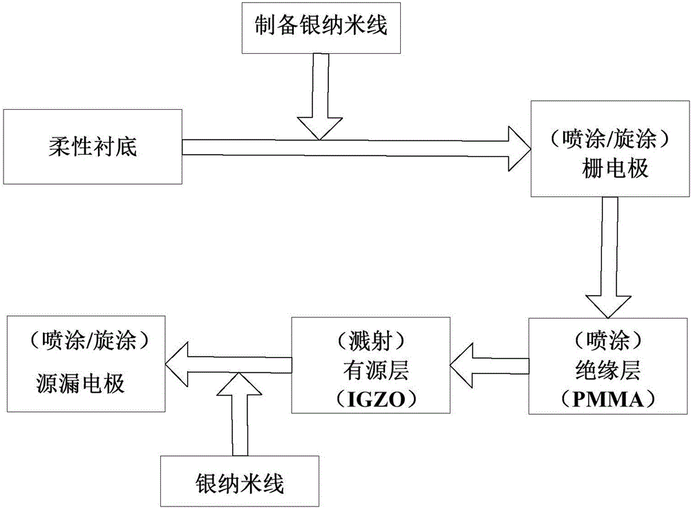
[0029] A method for preparing a flexible thin film transistor with a novel bottom gate structure, comprising the following steps:
[0030] Step 1. Prepare polydimethylsiloxane flexible substrate by spin coating method: mix polydimethylsiloxane main agent and hardener at a mass ratio of 10:1, and place in a vacuum environment of 0.1 Torr 10 to 30 minutes to remove air bubbles to obtain a polydimethylsiloxane spin-coating liquid; then spin-coat the above-mentioned polydimethylsiloxane spin-coating liquid on the silanized glass substrate; The glass substrate of dimethylsiloxane is dried at 60-80°C for 1-3 hours for curing and molding, and the cured and molding polydimethylsiloxane film is peeled off, and plasma oxygen treatment is performed to make the surface hydrophilic. water to obtain a polydimethylsiloxane flexible substrate with a thickness of 0.2-0.3 mm; finally, the polydimethylsiloxane film obtained after the plasma oxygen treatment in the previous step is sequentially h...
Embodiment 1
[0036] A method for preparing a flexible thin film transistor with a novel bottom gate structure, comprising the following steps:
[0037] Step 1. Prepare polydimethylsiloxane flexible substrate by spin coating method: mix polydimethylsiloxane main agent and hardener at a mass ratio of 10:1, and place in a vacuum environment of 0.1 Torr 30min to remove bubbles to obtain polydimethylsiloxane spin-coating liquid; then spin-coat the above-mentioned polydimethylsiloxane spin-coating liquid on the glass substrate after silanization treatment; The glass substrate of polydimethylsiloxane is dried at 80°C for 3 hours for curing and molding, and the cured and molding polydimethylsiloxane film is peeled off, and plasma oxygen treatment is performed to make the surface hydrophilic, and the thickness can be obtained. 0.2mm polydimethylsiloxane flexible substrate; finally, the polydimethylsiloxane film obtained after the plasma oxygen treatment in the previous step was ultrasonically clean...
Embodiment 2
[0043] A method for preparing a flexible thin film transistor with a novel bottom gate structure, comprising the following steps:
[0044] Step 1. Prepare polydimethylsiloxane flexible substrate by spin coating method: mix polydimethylsiloxane main agent and hardener at a mass ratio of 10:1, and place in a vacuum environment of 0.1 Torr 30min to remove bubbles to obtain polydimethylsiloxane spin-coating liquid; then spin-coat the above-mentioned polydimethylsiloxane spin-coating liquid on the glass substrate after silanization treatment; The glass substrate of polydimethylsiloxane is dried at 80°C for 3 hours for curing and molding, and the cured and molding polydimethylsiloxane film is peeled off, and plasma oxygen treatment is performed to make the surface hydrophilic, and the thickness can be obtained. 0.2mm polydimethylsiloxane flexible substrate; finally, the polydimethylsiloxane film obtained after the plasma oxygen treatment in the previous step was ultrasonically clean...
PUM
 Abstract
Description
Claims
Application Information
 - R&D
- Intellectual Property
- Life Sciences
- Materials
- Tech Scout
- Unparalleled Data Quality
- Higher Quality Content
- 60% Fewer Hallucinations
Browse by: Latest US Patents, China's latest patents, Technical Efficacy Thesaurus, Application Domain, Technology Topic, Popular Technical Reports.
© 2025 PatSnap. All rights reserved.Legal|Privacy policy|Modern Slavery Act Transparency Statement|Sitemap|About US| Contact US: help@patsnap.com