LCD (liquid crystal display) integral touch device with an external copper process

A liquid crystal display and touch device technology, applied in the input/output process of instruments, data processing, optics, etc., can solve the problems of large impedance, high impedance ratio, power consumption increase, etc., and achieve channel impedance reduction and touch response speed. , The effect of reducing power consumption

Inactive Publication Date: 2016-06-29
赵宗轩
View PDF4 Cites 4 Cited by
  • Summary
  • Abstract
  • Description
  • Claims
  • Application Information

AI Technical Summary

Problems solved by technology

[0003] The existing integrated touch device requires an ITO-coated metal conductive layer, and the sensing pattern layer is made of an ITO conductive layer to form a mutual capacitance. Due to the high impedance ratio of ITO, the requirements for the driving capability of the IC are also relatively high, and 2-3 driving ICs are used. In order to meet the touch signal processing, the problem is prominent in solving medium and large size touch drives. For example, in the case of flexible integrated touch devices, the impedance of ITO will become larger; increasing the pattern pitch and reducing the channel impedance will cause transmittance decrease, the power consumption will also increase

Method used


Image

  • LCD (liquid crystal display) integral touch device with an external copper process
  • LCD (liquid crystal display) integral touch device with an external copper process
  • LCD (liquid crystal display) integral touch device with an external copper process

Examples


Embodiment Construction

[0027] The present invention will be further elaborated below in conjunction with the embodiment given with accompanying drawing, but embodiment does not constitute any limitation to the present invention.

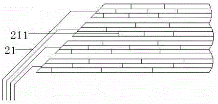
[0028] see figure 1 , an LCD liquid crystal display integrated touch device with external copper process, consisting of a four-layer structure of an upper glass substrate 1, a first metal grid conductive layer 2, an OC insulating layer 3, and a second metal grid conductive layer 4, the upper glass The flexible transparent substrate selected for substrate 1 is one of polymethyl methacrylate, polyurethane and polycarbonate; the OC insulating layer 3 is composed of PI substrate and high insulating material, and is directly coated on the first metal Grid conductive layer 2.

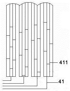
[0029] see figure 1 , figure 2 The first metal grid conductive layer 2 is a layer of metal copper by low-temperature sputtering, and the first metal grid lines 21 are directly formed by exposure and o...


PUM


Abstract

The invention relates to an integrated touch device with an external copper process for an LCD liquid crystal display. It includes an upper glass substrate and a sensing pattern layer; the surface of the upper glass substrate is copper plated with a first metal grid conductive layer, the first metal grid conductive layer is coated with an OC insulating layer, and the copper on the OC insulating layer is plated with a second metal grid conductive layer; the first metal grid conductive layer directly forms the first metal grid circuit, and forms the electroplating driving electrode pattern through the driving electrode unit; the second metal grid conductive layer directly forms the second metal grid circuit, and forms the second metal grid circuit directly through the driving electrode unit The sensing electrode unit forms an electroplating sensing electrode pattern; the electroplating driving electrode pattern and the electroplating sensing electrode pattern constitute the distribution of the sensing pattern layer. The present invention can reduce channel impedance, reduce power consumption, and improve transmittance without reducing pitch; in the case of a flexible integrated touch device, it can reduce the change of impedance when bending or stretching.

Description

technical field [0001] The invention relates to an integrated touch device, in particular to an integrated touch device with an external copper process for an LCD liquid crystal display. Background technique [0002] With the development of ultra-thin and large-screen mobile phones, and the demand for touch screens in tablets and ultrabooks, touch screen technology is undergoing rapid evolution, and new technologies are becoming mature. New TOL, mutual-capacity single-layer multi-touch, Oncell / Technologies such as Incell and flexible display will become the trend in the future, and major manufacturers are also investing in the development of reliable Oncecell touch screens. In addition, with the application of TSP technology to flexible display devices, the touch screen panel on the front surface of the display device of the organic light emitting display or liquid crystal display is also increasingly becoming a research direction for display touch. [0003] The existing i...

Claims


Application Information

Patent Timeline
Patent Type & Authority Applications(China)
IPC IPC(8): G02F1/1333G06F3/041G06F3/044
CPCG02F1/13338G06F3/0412G06F2203/04112
Inventor 赵宗轩王泊可熊元伟
Owner 赵宗轩
Why Eureka
Try Eureka