
Preparation method of micro lens nanopore hybrid array structure

A technology of microlens array and hybrid structure, applied in the directions of lenses, instruments, optics, etc., can solve the problems of insurmountable surface mechanical properties, high preparation cost, unsuitability, etc., and achieve the effects of flexible and diverse methods, time saving, and efficiency improvement.

Inactive Publication Date: 2016-06-15
中灿智能科技(沭阳)有限公司
View PDF7 Cites 6 Cited by
  • Summary
  • Abstract
  • Description
  • Claims
  • Application Information

AI Technical Summary

Problems solved by technology

However, they still use polydimethylsiloxane soft nanoimprint templates, which are expensive to prepare and are not suitable for large-area industrial roll-to-roll printing.
Moreover, although the sub-wavelength nano-array structure is realized on the micro-lens array to form a micro-nano hybrid structure, the nano-array structure is still on the surface of the micro-lens array, which still cannot overcome the defects of weak surface mechanical properties and easy scratches.

Method used


Image

  • Preparation method of micro lens nanopore hybrid array structure
  • Preparation method of micro lens nanopore hybrid array structure
  • Preparation method of micro lens nanopore hybrid array structure

Examples


Embodiment Construction

[0061] The present invention will be described in detail below in conjunction with the accompanying drawings and specific embodiments. However, these embodiments do not limit the present invention, and the structural, method or functional changes made by those skilled in the art according to these specific embodiments without creative work shall be included in the protection scope of the present invention .

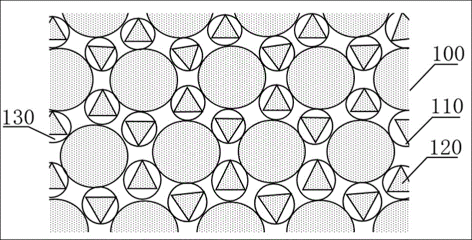
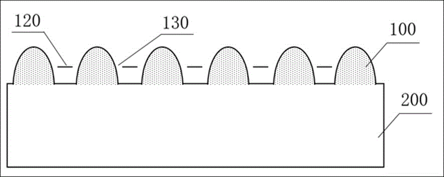
[0062] The invention discloses a preparation method of a microlens nanohole mixed structure. see figure 1 , figure 2 As shown, the structure includes materials made of UV-curable adhesive: microlens array 100, micron hole array 110 nested between the microlens arrays, micron triangular array 120 embedded in the micron hole array, micron hole array The nanohole-like array 130 and the base 220 with optional materials are formed with the interval regions embedded with micron triangles.

[0063] The structure of each part in the present invention will be described in det...


PUM

PropertyMeasurementUnit
Diameteraaaaaaaaaa

Abstract

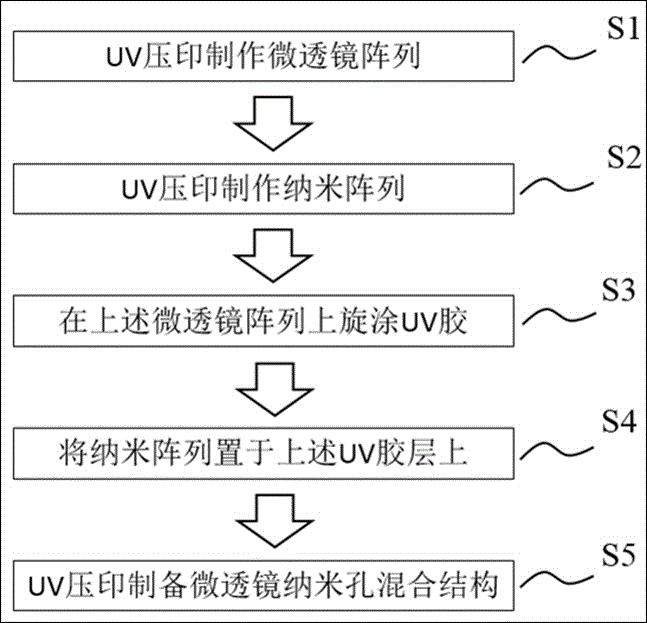
The invention discloses a preparation method of a micro lens nanopore hybrid array structure. The preparation method comprises the steps of: firstly, preparing a micro lens array made of ultraviolet curing adhesive by adopting an ultraviolet nano-imprinting method; secondly, preparing a nano array template made of urethane acrylate through ultraviolet nano-imprinting; and finally painting ultraviolet light curing adhesive on the micro lens array, and preparing the micro lens nanopore hybrid array structure made of the ultraviolet light curing adhesive through ultraviolet nano-imprinting by utilizing the nano array template. The micro lens nanopore hybrid array structure is composed of the micro lens array, micron circular holes embedded in the periphery of micro lenses, micron triangles internally embedded in the micron circular holes, and nano holes formed in spaced regions among the micron circular holes and the micron triangles. The micro lens nanopore hybrid array structure overcomes the defects that the micro lens array cannot inhibit reflection of surface incidence light rays effectively and the surface mechanical performance of the nano array is weak at the same time; meanwhile, the technology is low in cost and simple in preparation, and the large-area batched preparation can be achieved.

Description

technical field [0001] The invention relates to the fields of micro-nano structure and device preparation and ultraviolet nano-imprint photolithography processing, in particular to a micro-nano preparation method of a micro-lens nano-hole hybrid structure. Background technique [0002] As a very important micro-nano structured optical component, microlens array has many unique optical properties. By precisely controlling parameters such as microlens distribution, focal length, duty cycle, and numerical aperture, optical modulation such as diffusion, shaping, focusing, and imaging of the incident beam can be realized. Therefore, it is more and more widely used in the fields of focal plane light collection, large-area display, laser collimation, optical computing, optical efficiency enhancement, and optical interconnection. Moreover, the technology of preparing microlens arrays on hard materials (such as quartz, glass, etc.) and soft materials (such as polybutylmethacrylate, ...

Claims


Application Information

Patent Timeline
IPC IPC(8): G02B3/00
CPCG02B3/0018G02B3/0031
Inventor 周雷范媛媛高本领毛安君蒋青松胡光
Owner 中灿智能科技(沭阳)有限公司
Learn More