Full-graphene group flexible organic field-effect transistor and manufacturing method thereof
A manufacturing method and graphene technology, which is applied in semiconductor/solid-state device manufacturing, photovoltaic power generation, electrical components, etc., can solve the problems of high production equipment and process control requirements, difficult control of single crystal thin film growth, and difficulty in achieving product yield, etc. problems, to achieve stable electrical performance, low requirements for production equipment, and strong water and oxygen resistance
- Summary
- Abstract
- Description
- Claims
- Application Information
AI Technical Summary
Problems solved by technology
Method used
Image
Examples
Embodiment 1
[0048] 1.1 as Figure 6-1 and 6-2 , choose PI with a thickness of 90 μm, scrub the PI with detergent powder and cut it into 2cm×2.5cm, and then ultrasonically clean it with acetone, ethanol, and deionized water for 10 minutes respectively;
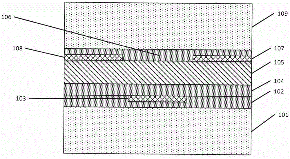
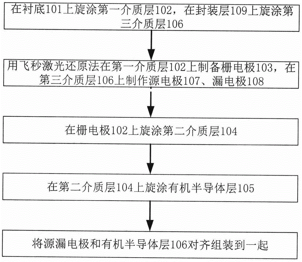
[0049] 1.2 After drying with nitrogen, the surface of PI was treated with oxygen plasma to make the surface hydrophilic, and the preparation of 101 and 109 was completed.
Embodiment 2
[0051] 2.1 Weigh 30mg of purified graphene oxide powder with an electronic scale, weigh 60ml of ethanol with a measuring cylinder, and mix the two in a glass bottle;
[0052] 2.2 Seal the above-mentioned glass vial and place it on a magnetic stirrer for 2 hours to prepare a 15 mg / ml solution.
Embodiment 3
[0054] 3.1 as Figure 6-3 and 6-4 As shown, turn on the mechanical pump of the glue homogenizer, and set the parameters of the glue homogenizer: low speed rotation 400 rpm, 4 seconds, high speed rotation 1000 rpm, 50 seconds;
[0055] 3.2 Put 101 and 109 in Example 1 on the tip respectively, press the suction piece, pipette 40 μl of the graphene oxide solution in Example 2 and drop it on 101 and 109, close the lid and start spin coating ;
[0056] 3.3 After the spin coating is finished, put the spin-coated 101 and 109 into a vacuum drying oven, evacuate to 0.09Pa, set the temperature at 70°C, and dry for 2 hours to complete the preparation of 102 and 106. After testing with a step meter The film thickness of 102 and 106 is 20nm;
PUM
| Property | Measurement | Unit |
|---|---|---|
| thickness | aaaaa | aaaaa |
| thickness | aaaaa | aaaaa |
| length | aaaaa | aaaaa |
Abstract
Description
Claims
Application Information
 - R&D
- Intellectual Property
- Life Sciences
- Materials
- Tech Scout
- Unparalleled Data Quality
- Higher Quality Content
- 60% Fewer Hallucinations
Browse by: Latest US Patents, China's latest patents, Technical Efficacy Thesaurus, Application Domain, Technology Topic, Popular Technical Reports.
© 2025 PatSnap. All rights reserved.Legal|Privacy policy|Modern Slavery Act Transparency Statement|Sitemap|About US| Contact US: help@patsnap.com


