
Multi-chip upright stack sandwich package structure with exposed frame and technique for multi-chip upright stack sandwich package structure

A technology of packaging structure and process method, which is applied in the manufacturing of electrical components, electric solid-state devices, semiconductor/solid-state devices, etc., can solve the problems of poor welding, low manufacturing efficiency, welding dumping, etc., and achieves reduced packaging resistance, improved production efficiency, The effect of reducing the interconnection process

Inactive Publication Date: 2016-05-04
JCET GROUP CO LTD
View PDF3 Cites 1 Cited by
  • Summary
  • Abstract
  • Description
  • Claims
  • Application Information

AI Technical Summary

Problems solved by technology

[0013] 1.) In this MOS package structure, the drain, source and gate of the chip and the lead frame are connected to each other by using different equipment, the process is complicated, and the purchase cost of the equipment is high
[0014] 2.) When this MOS packaging structure couples the metal splint and the metal bonding wire to the chip and the pin, it can only be carried out one by one, and the whole piece cannot be integrally formed, and the manufacturing efficiency is low.
[0015] 3.) The internal and external pins of this MOS package are not integrally formed, but welded by solder, so there is still a high contact resistance at the junction of the internal and external pins (that is, the contact between the metal splint, the metal strip and the lead frame)
[0016] 4.) When using a metal splint to couple to the chip and the metal pin, because of the different chip board or chip area, the metal splint and the punching and handling mold and mechanism of the metal splint must be redesigned and redesigned. Manufacturing, and these changes often result in waste of acquisition money, waste of re-architecting time costs, waste of business opportunity costs, and waste of staffing
[0017] 5.) When using a metal splint to couple to the chip and metal pins, because the metal splint is very small, during the production punching, handling and welding process, the metal splint often falls during transportation, falls during welding, and poor welding. Damage to yield and reliability

Method used

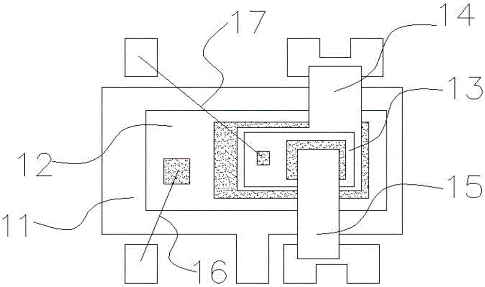
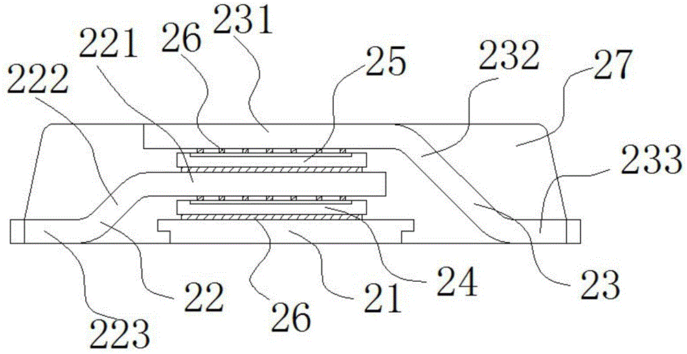
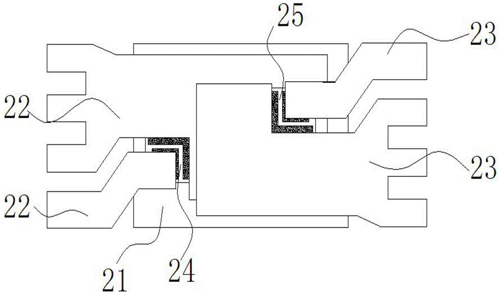

Image

  • Multi-chip upright stack sandwich package structure with exposed frame and technique for multi-chip upright stack sandwich package structure
  • Multi-chip upright stack sandwich package structure with exposed frame and technique for multi-chip upright stack sandwich package structure
  • Multi-chip upright stack sandwich package structure with exposed frame and technique for multi-chip upright stack sandwich package structure

Examples


Embodiment Construction

[0079] The present invention will be further described in detail below in conjunction with the accompanying drawings and embodiments.

[0080] As shown in Fig. 8(a) to Fig. 8(n), a process method of a frame-exposed multi-chip stacked sandwich packaging structure in this embodiment, the specific process steps are as follows:

[0081] Step 1, see Figure 8 (a), provide the first lead frame, the material of the first lead frame is alloy copper material, pure copper material, aluminum copper plated material, zinc plated copper material, nickel-iron alloy material, or other CTE The range is 8*10^-6 / ℃~25*10^-6 / ℃ conductive material;

[0082] Step 2, see Figure 8(b), apply solder paste on the base island area of ​​the first lead frame by screen printing, the purpose is to realize the bonding with the base island after the first chip is implanted. Thickness and opening area can precisely control the thickness, area and position of solder paste;

[0083] Step 3, referring to FIG. 8(c)...


PUM


Abstract

The invention relates to a multi-chip upright stack sandwich package structure with an exposed frame and a technique for the multi-chip upright stack sandwich package structure. The technique comprises the following steps: (1) providing a first lead frame; (2) coating the first lead frame with a solder paste; (3) implanting a first chip into the solder paste of the first lead frame; (4) providing a second lead frame; (5) coating the second lead frame with the solder paste; (6) laminating the second lead frame on the first chip; (7) carrying out reflow soldering; (8) coating the second lead frame with the solder paste; (9) implanting a second chip into the second lead frame; (10) providing a third lead frame; (11) coating the third lead frame with the solder paste; (12) laminating the third lead frame on the second chip; (13) carrying out reflux soldering; (14) carrying out plastic package by a molding compound; and (15) carrying out cutting or punching operation. The technique has the beneficial effects that the heat dissipation capacity of a product is improved and the package resistance of the product is reduced.

Description

technical field [0001] The invention relates to a frame-exposed multi-chip stacked sandwich packaging structure and a process method thereof, belonging to the technical field of semiconductor packaging. Background technique [0002] In recent years, with the continuous pursuit of power density in electronic products, whether it is Diode (secondary tube) or Transistor (transistor) packaging, especially the MOS products in Transistor are moving towards higher power, smaller size, faster , The trend of better heat dissipation is developing. The one-time manufacturing method of packaging is also gradually sprinting and challenging from single-chip packaging technology to high-density, high-difficulty and low-cost one-time packaging technology in small areas or even larger areas. [0003] Therefore, the packaging of MOS products has been improved in terms of various electrical properties such as parasitic resistance, capacitance, and inductance, packaging structure, heat dissipa...

Claims


Application Information

Patent Timeline
Patent Type & Authority Applications(China)
IPC IPC(8): H01L21/56H01L23/31H01L23/495
CPCH01L21/56H01L23/3114H01L23/49534H01L2224/32245H01L2224/48247H01L2224/97H01L2924/181H01L2924/00012
Inventor 刘恺梁志忠张波王亚琴
Owner JCET GROUP CO LTD
Learn More