Method of forming semiconductor structure

A semiconductor and transistor technology, which is applied in the field of semiconductor structure formation, can solve the problems of metal interconnect structure resistance drift, increase of parasitic capacitance of metal interconnect structure, and reduce electrical performance of semiconductor devices, so as to optimize device electrical performance and increase bottom area, the effect of increasing the effective contact area

Inactive Publication Date: 2016-03-30
SEMICON MFG INT (SHANGHAI) CORP
View PDF4 Cites 7 Cited by
  • Summary
  • Abstract
  • Description
  • Claims
  • Application Information

AI Technical Summary

Problems solved by technology

Before the feature size of the metal interconnection structure is reduced, the current process technology has no obvious adverse effects on the metal interconnection structure, but the continuous reduction of the feature size has brought great challenges to the process technology, and the resistance value of the metal interconnection structure is prone to drift And the problem of increased parasitic capacitance of metal interconnection structure, these problems will reduce the electrical performance of semiconductor devices

Method used


Image

  • Method of forming semiconductor structure
  • Method of forming semiconductor structure
  • Method of forming semiconductor structure

Examples


Embodiment Construction

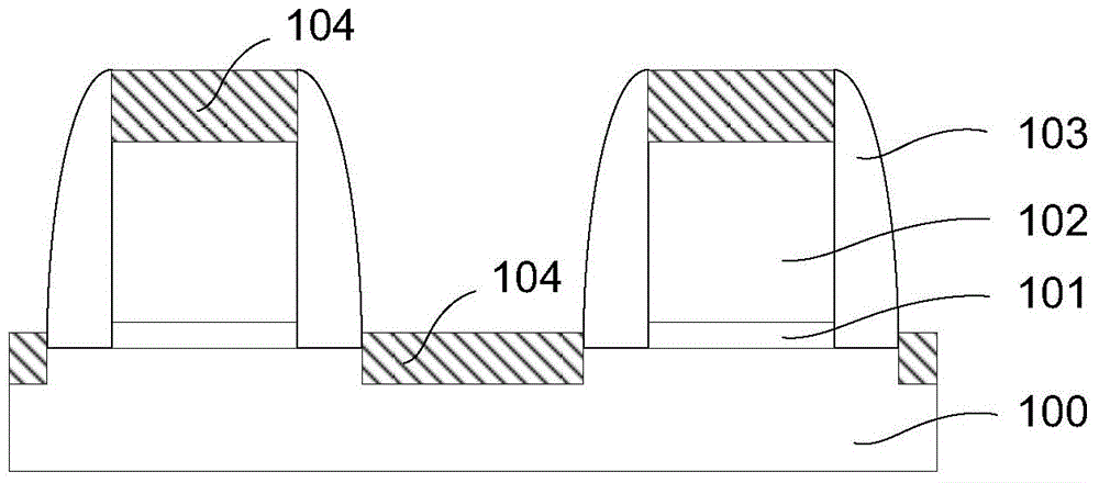
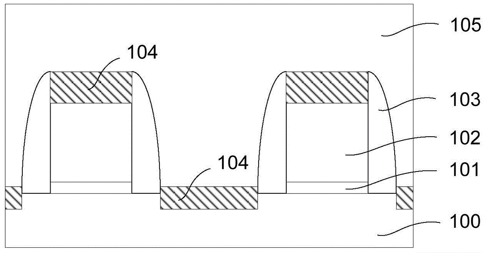
[0030] It can be seen from the background technology that with the continuous reduction of semiconductor feature size, the metal interconnection structure needs to perform high-performance and high-density connections in multi-layer and complex wiring layers, which brings great challenges to the manufacturing process of the metal interconnection structure. Not a small challenge, there are problems of resistance value drift and parasitic capacitance increase, which reduces the electrical performance of the device.

[0031] The research on the metal interconnection structure and its manufacturing process in the prior art found that: when forming the trench for filling the metal to obtain the wiring layer, the existing dry etching process is easy under the smaller mask opening. The cross-sectional shape of the groove with a relatively inclined side wall is formed. The groove shape will cause a serious reduction in the size of the bottom of the wiring layer, resulting in a decrease...


PUM


Abstract

The invention provides a method of forming a semiconductor structure. The method comprises the steps of providing a semiconductor substrate with a transistor forming on the surface thereof; forming a first interlayer dielectric layer covering the semiconductor substrate and the transistor; forming a plug in the first interlayer dielectric layer; forming a sacrificial layer covering the first interlayer dielectric layer and the plug; etching the sacrificial layer, and forming a first trench in the sacrificial layer; forming a second interlayer dielectric layer filled in the first trench; removing the remaining sacrificial layer, and forming a second trench which exposes the surface of the plug; and forming a wiring layer filled in the second trench, the bottom of the wiring layer being electrically connected with the plug and the top of the wiring layer having a size smaller or equal to that of the bottom. The effective contact area between the wiring layer and the plug is increased, the resistance drift phenomenon of a metal interconnect structure is improved, damage to the interlayer dielectric layers from the etching process is avoided, the parasitic capacitance is reduced, and the device electrical performance is optimized.

Description

technical field [0001] The invention relates to the field of semiconductor manufacturing, in particular to a method for forming a semiconductor structure. Background technique [0002] With the increasing development of semiconductor integrated circuits, the circuit density inside the semiconductor integrated circuit is increasing, and the number of components contained is also increasing. In semiconductor integrated circuits, metal oxide semiconductor (MetalOxideSemiconductor, MOS) transistors are one of the most important components. With the increasing performance requirements of semiconductor devices in the market, the size of semiconductor devices is becoming smaller and smaller. The manufacturing process of devices has brought many improvements and challenges, and small process deviations will lead to changes in the electrical properties of semiconductor devices. [0003] As an integral part of semiconductor devices, the metal interconnection structure includes wiring...

Claims


Application Information

Patent Timeline
Patent Type & Authority Applications(China)
IPC IPC(8): H01L21/768
Inventor 李凤莲
Owner SEMICON MFG INT (SHANGHAI) CORP
Why Eureka
Try Eureka