Trench-gate AlGaN/GaN HEMT device structure and manufacturing method

A technology of devices and trench gates, which is applied to the structure and manufacture of AlGaN/GaN HEMT devices with floating gate composite field plate trench gates, and in the field of AlGaN/GaN high electron mobility transistors, which can solve the problems of withstand voltage, on-resistance and frequency characteristics. Practical application and other issues, to achieve the effect of reducing the peak value of the electric field, reducing the on-resistance, and increasing the control ability

Inactive Publication Date: 2016-02-24
XIDIAN UNIV
View PDF8 Cites 9 Cited by
  • Summary
  • Abstract
  • Description
  • Claims
  • Application Information

AI Technical Summary

Problems solved by technology

[0006] However, the current AlGaN / GaN HEMT devices cannot meet the needs of practical applications in terms of withstand voltage, on-resistance and frequency characteristics.

Method used


Image

  • Trench-gate AlGaN/GaN HEMT device structure and manufacturing method
  • Trench-gate AlGaN/GaN HEMT device structure and manufacturing method

Examples


Embodiment Construction

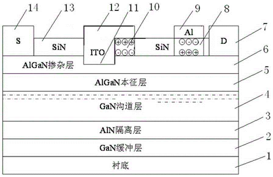
[0036] refer to figure 1 , a floating-gate compound field plate trench gate AlGaN / GaN HEMT device structure of the present invention, comprising a substrate 1, a GaN buffer layer 2, an AlN isolation layer 3, a GaN channel layer 4, an intrinsic AlGaN layer 5, and an AlGaN doped layer 6. PTFE organic insulating medium layer 10 and LiF layer 8, ITO gate field plate 12, Al floating field plate 9, passivation layer 13, gate, drain electrode 7 and source electrode 14. The device structure from bottom to top is: substrate 1, GaN buffer layer 2, AlN isolation layer 3, GaN channel layer 4, intrinsic AlGaN layer 5, AlGaN doped layer 6, on which AlGaN doped layer 6 is set The active electrode 14, the drain electrode 7, the organic insulating medium layer 10, the LiF layer 8, the ITO gate field plate 12 and the passivation layer 13, the source electrode 14 and the drain electrode 7 are arranged at both ends above the AlGaN doped layer 6, The LiF layer 8 is close to the drain electrode 7,...


PUM


Abstract

The invention discloses a composite gate floating field plate trench-gate AlGaN / GaN HEMT device structure and a manufacturing method thereof. The composite gate floating field plate trench-gate AlGaN / GaN HEMT device structure comprises a substrate, a GaN buffer layer, an AlN isolating layer, a GaN channel layer, an intrinsic AlGaN layer and an AlGaN doped layer which are sequentially compounded from bottom to top, wherein both ends on the AlGaN doped layer are respectively provided with a source and a drain, a LiF layer is arranged on the AlGaN doped layer at a position close to the drain, and a floating field plate is arranged on the LiF layer; an organic insulating dielectric layer is arranged between the LiF layer and the source, and a gate field plate is arranged on and beside the organic insulating dielectric layer; and a passivation layer is arranged in a bare area on the AlGaN doped layer. According to the trench-gate AlGaN / GaN HEMT device structure and the manufacturing method thereof, the breakdown voltage of a device is increased by utilizing the PTFE layer and the ITO gate field plate, the on resistance between the gate and the source of the device is decreased by utilizing the LiF layer and the Al floating field plate, and the breakdown voltage of the device is further increased by utilizing the gate field plate and the floating field plate.

Description

technical field [0001] The invention belongs to the field of microelectronics technology, and relates to the manufacture of semiconductor devices, in particular to a structure and a manufacturing method of an AlGaN / GaN HEMT device with a floating gate composite field plate groove grid, which can be used to manufacture high breakdown voltage, low on-resistance and high AlGaN / GaN high electron mobility transistors with frequency characteristics. technical background [0002] In recent years, the third-generation wide-bandgap semiconductors represented by SiC and GaN have been widely recognized for their characteristics such as large bandgap, high breakdown electric field, high thermal conductivity, high saturated electron velocity, and high two-dimensional electron gas concentration at the heterojunction interface. focus on. In theory, high electron mobility transistor HEMT, light emitting diode LED, laser diode LD and other devices made of these materials are more superior...

Claims


Application Information

Patent Timeline
Patent Type & Authority Applications(China)
IPC IPC(8): H01L29/78H01L29/10H01L29/40H01L21/336
CPCH01L29/78H01L29/1066H01L29/402H01L29/408H01L29/4236H01L29/42364H01L29/66477
Inventor 柴常春杨琦陈鹏远杨银堂刘阳樊庆扬于新海史春蕾孙斌
Owner XIDIAN UNIV
Why Eureka
Try Eureka