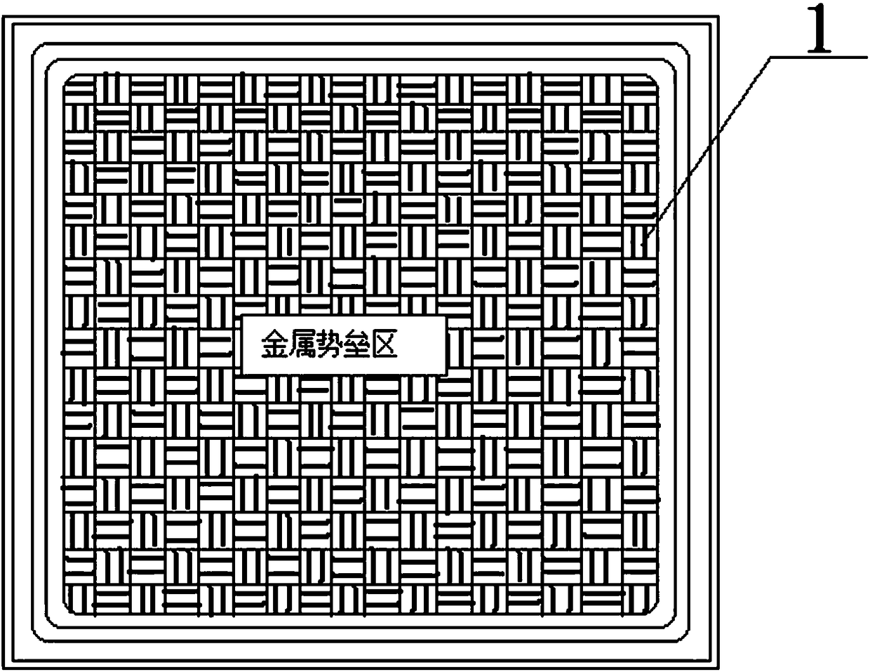
A kind of manufacturing method of 100v schottky diode mesa
A technology of Schottky diode and manufacturing method, applied in semiconductor/solid-state device manufacturing, semiconductor device, electrical components and other directions, can solve the problems of forward voltage drop, low junction temperature, large forward voltage drop, etc., to reduce leakage Effects of current and forward voltage drop, increasing metal area, reducing forward voltage drop
- Summary
- Abstract
- Description
- Claims
- Application Information
AI Technical Summary
Problems solved by technology
Method used
Image
Examples
Embodiment 1
[0030] A method for manufacturing a 100V Schottky diode mesa, comprising the following steps:
[0031] (1) Use cleaning solution I and cleaning solution II in sequence to clean the substrate silicon wafer at a temperature of 70°C, and dry it for later use. The cleaning solution I is made of NH 3 h 2 O, H 2 o 2 and H 2 O is mixed according to the volume ratio of 1:1:5, and the cleaning solution II is composed of HCL, H 2 o 2 and H 2 O is mixed according to the volume ratio of 1:1:5;
[0032] (2) Perform initial oxidation on the cleaned substrate silicon wafer, and the thickness of the oxide layer is 6800Å;
[0033] (3) Perform base photolithography on the front side of the oxidized substrate silicon wafer, implant boron on the P+ ring of the substrate silicon wafer, and then perform annealing treatment;
[0034] (4) Conduct lead hole photolithography on the annealed substrate silicon wafer;
[0035] (5) Carry out mesa lithography on the mesa of the barrier area of th...
Embodiment 2
[0043] A method for manufacturing a 100V Schottky diode mesa, comprising the following steps:
[0044] (1) Use cleaning solution I and cleaning solution II in sequence to clean the substrate silicon wafer at a temperature of 75 ° C, and dry it for later use. The cleaning solution I is made of NH 3 h 2 O, H 2 o 2 and H 2 O is mixed according to the volume ratio of 1:1:5, and the cleaning solution II is composed of HCL, H 2 o 2 and H 2 O is mixed according to the volume ratio of 1:1:5;
[0045](2) Perform initial oxidation on the cleaned substrate silicon wafer, and the thickness of the oxide layer is 7000Å;
[0046] (3) Perform base photolithography on the front side of the oxidized substrate silicon wafer, implant boron on the P+ ring of the substrate silicon wafer, and then perform annealing treatment;
[0047] (4) Conduct lead hole photolithography on the annealed substrate silicon wafer;
[0048] (5) Carry out mesa lithography on the mesa of the barrier area of t...
Embodiment 3
[0056] A method for manufacturing a 100V Schottky diode mesa, comprising the following steps:
[0057] (1) Use cleaning solution I and cleaning solution II in sequence to clean the substrate silicon wafer at a temperature of 80°C, and dry it for later use. The cleaning solution I is made of NH 3 h 2 O, H 2 o 2 and H 2 O is mixed according to the volume ratio of 1:1:5, and the cleaning solution II is composed of HCL, H 2 o 2 and H 2 O is mixed according to the volume ratio of 1:1:5;
[0058] (2) Perform initial oxidation on the cleaned substrate silicon wafer, and the thickness of the oxide layer is 7200Å;
[0059] (3) Perform base photolithography on the front side of the oxidized substrate silicon wafer, implant boron on the P+ ring of the substrate silicon wafer, and then perform annealing treatment;
[0060] (4) Conduct lead hole photolithography on the annealed substrate silicon wafer;
[0061] (5) Carry out mesa lithography on the mesa of the barrier area of th...
PUM
| Property | Measurement | Unit |
|---|---|---|
| thickness | aaaaa | aaaaa |
| thickness | aaaaa | aaaaa |
| thickness | aaaaa | aaaaa |
Abstract
Description
Claims
Application Information
 - R&D Engineer
- R&D Manager
- IP Professional
- Industry Leading Data Capabilities
- Powerful AI technology
- Patent DNA Extraction
Browse by: Latest US Patents, China's latest patents, Technical Efficacy Thesaurus, Application Domain, Technology Topic, Popular Technical Reports.
© 2024 PatSnap. All rights reserved.Legal|Privacy policy|Modern Slavery Act Transparency Statement|Sitemap|About US| Contact US: help@patsnap.com


