Low insertion loss self-biased microstrip circulator based on magnetic nanowire array
A nanowire array, insertion loss technology, applied in waveguide-type devices, circuits, electrical components, etc., can solve problems such as large insertion loss, and achieve the effects of low insertion loss, high isolation, and lower dielectric constant
- Summary
- Abstract
- Description
- Claims
- Application Information
AI Technical Summary
Problems solved by technology
Method used
Image
Examples
Embodiment
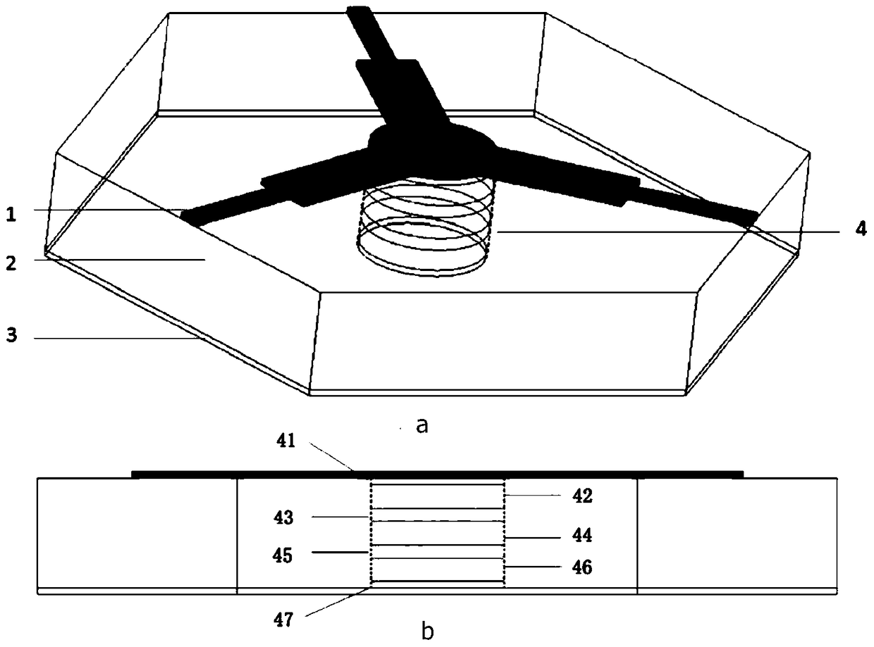
[0023] This embodiment includes microstrip Y-junction matching line 1, hexagonal prism dielectric layer 2 with a cylindrical through hole in the center, metal bottom electrode 3 and multi-layer cylindrical central junction 4 composed of four major parts. The central junction is a multi-layer structure, the upper and lower layers are insulating layers, and the middle is an array layer of three layers of Fe nanowires deposited with a porous alumina template. The three-layer array layers are separated by two layers of air layers. Neglected spacers to support the entire structure.
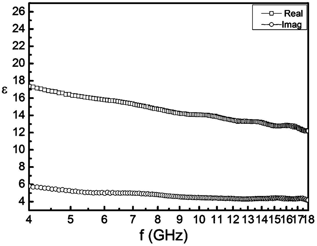
[0024] The nanowires used in the present invention are prepared by depositing Fe nanowires in a porous alumina template with a thickness of 70um, a nanopore diameter of about 80nm, and a void ratio of 60% by the electrochemical deposition method, and the measured length of the nanowires is about 60um, the remanence (4πMr) is 4200gauss, the high frequency spectrum of magnetic permeability and high frequ...
PUM
 Abstract
Description
Claims
Application Information
 - R&D
- Intellectual Property
- Life Sciences
- Materials
- Tech Scout
- Unparalleled Data Quality
- Higher Quality Content
- 60% Fewer Hallucinations
Browse by: Latest US Patents, China's latest patents, Technical Efficacy Thesaurus, Application Domain, Technology Topic, Popular Technical Reports.
© 2025 PatSnap. All rights reserved.Legal|Privacy policy|Modern Slavery Act Transparency Statement|Sitemap|About US| Contact US: help@patsnap.com


