Semiconductor element and preparation method thereof
A semiconductor and N-type semiconductor technology, which is applied in semiconductor devices, semiconductor/solid-state device manufacturing, electrical components, etc., can solve problems such as core grain electrical anomalies, lower production yields, chemical solution corrosion, etc., to release stress and improve Corrosion resistance, the effect of enhancing corrosion resistance
- Summary
- Abstract
- Description
- Claims
- Application Information
AI Technical Summary
Problems solved by technology
Method used
Image
Examples
Embodiment 1
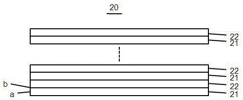
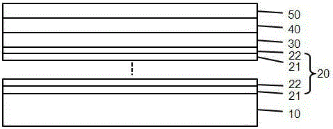
[0038] See attached Figure 1~2 , a semiconductor element in the present invention, comprising a substrate 10, a buffer layer 20, an N-type semiconductor layer 30, a light-emitting layer 40, and a P-type semiconductor layer 50, wherein the buffer layer 20 is at least composed of al x N 1-x Layer 21 and a thickness of 5 to 500 Angstroms of Al y o 1-y Layer 22 (0x N 1-x The thickness of layer 21 ≥ Al y o 1-y Layer 22 thickness. It was found experimentally that when Al x N 1-x Layer 21 thickness vs. Al y o 1-y The larger the thickness ratio of the layer 22 is, the better the lattice quality of the buffer layer 20 is. In the structure of the present invention, the use of Al x N 1-x Layer 21 and Al y o 1-y The superlattice structure of the layer 22 forms the buffer layer 20, which reduces the degree of corrosion of the sidewall by the chemical solution during the sidewall corrosion process of the subsequent chip manufacturing process, and improves the chip yield.
...
Embodiment 2
[0046] See attached image 3 , The difference between this embodiment and Embodiment 1 is that the buffer layer 20 of the present invention includes Al with a thickness of 5-500 angstroms. x N 1-x Layer 21 and a thickness of 5 to 500 Angstroms of Al y o 1-y layer 22 (0x N 1-x Layer 21 placed in Al y o 1-y Between the layer 22 and the substrate 10, the number of cycles of the superlattice structure layer ≥ 2, Al x N 1-x The thickness of layer 21 ≥ Al y o 1-y Layer 22 thickness.
[0047] The difference between the preparation method adopted in this embodiment and the preparation method in Example 1 is: S2. Put the substrate 10 into the chamber of a PVD machine, and deposit Al with a thickness of 5 to 500 angstroms on the surface of the substrate 10 by using the PVD method. x N 1-x Layer 21 and a thickness of 5 to 500 Angstroms of Al y o 1-y layer 22 (0x N 1-x layer 21, again in Al x N 1-x Deposit Al on the surface of layer 21 y o 1-y The layer 22 is stacked in ...
Embodiment 3
[0049] See attached Figure 4 The difference between this embodiment and Embodiment 1 is that a non-doped semiconductor layer 60 is deposited between the buffer layer 20 and the N-type semiconductor layer 30, and this layer is used to further improve the crystal quality of the subsequent epitaxial layer and improve the photoelectric performance of the semiconductor element. .
PUM
| Property | Measurement | Unit |
|---|---|---|
| wavelength | aaaaa | aaaaa |
| thickness | aaaaa | aaaaa |
Abstract
Description
Claims
Application Information
 - Generate Ideas
- Intellectual Property
- Life Sciences
- Materials
- Tech Scout
- Unparalleled Data Quality
- Higher Quality Content
- 60% Fewer Hallucinations
Browse by: Latest US Patents, China's latest patents, Technical Efficacy Thesaurus, Application Domain, Technology Topic, Popular Technical Reports.
© 2025 PatSnap. All rights reserved.Legal|Privacy policy|Modern Slavery Act Transparency Statement|Sitemap|About US| Contact US: help@patsnap.com


