Ultraviolet detector based on palladium/tin dioxide/silicon heterojunction and preparation method thereof

A tin dioxide and silicon heterojunction technology, used in semiconductor devices, final product manufacturing, sustainable manufacturing/processing, etc., can solve the problems of difficult preparation technology, inability to be popularized and applied, and expensive single crystal semiconductor thin film equipment. , to achieve the effect of suitable for mass production, short recovery time and easy integration

Pending Publication Date: 2016-01-13
CHINA UNIV OF PETROLEUM (EAST CHINA)
View PDF4 Cites 3 Cited by
  • Summary
  • Abstract
  • Description
  • Claims
  • Application Information

AI Technical Summary

Problems solved by technology

Single crystal thin films such as silicon carbide, gallium nitride, zinc oxide and other materials have also begun to be put into production, but due to the expensive equipment required to grow single crystal semiconductor thin films, and in view of the current single crystal growth technology, the preparation process is still very difficult cannot be popularized and applied

Method used


Image

  • Ultraviolet detector based on palladium/tin dioxide/silicon heterojunction and preparation method thereof
  • Ultraviolet detector based on palladium/tin dioxide/silicon heterojunction and preparation method thereof
  • Ultraviolet detector based on palladium/tin dioxide/silicon heterojunction and preparation method thereof

Examples


Embodiment 1

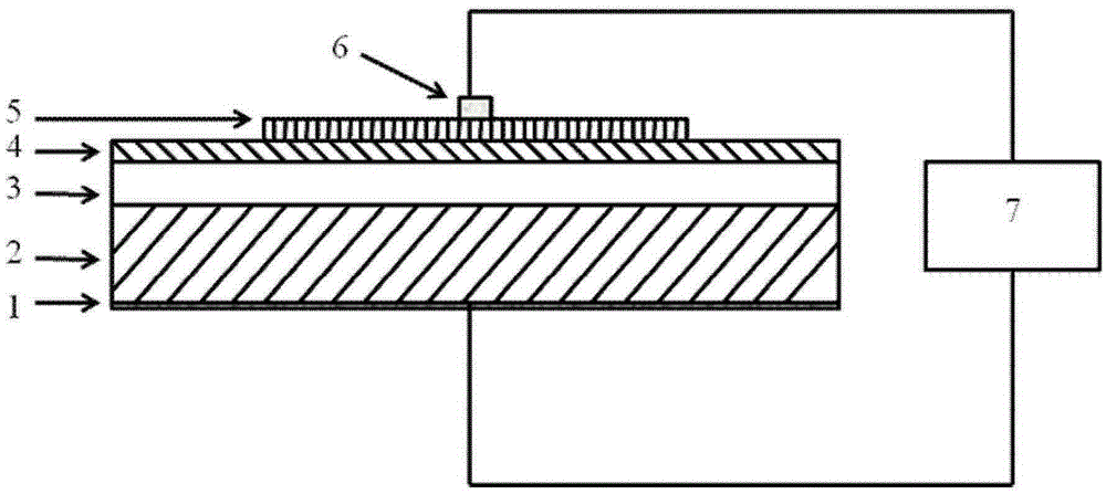
[0025] We selected a p-type monocrystalline silicon wafer with a thickness of 0.5 mm as the substrate, and retained its natural oxide layer. Clean the silicon wafer in ultrasonic wave with deionized water for 10 minutes, then wash the silicon wafer in ultrasonic wave with acetone for 1 hour, and finally clean the silicon wafer with absolute ethanol for 0.5 hour.

[0026] Tin dioxide film was prepared by DC magnetron sputtering: put the cleaned silicon substrate into the sputtering chamber, and turn on the vacuum system for vacuuming; when the background vacuum was 2.0×10 -4 At Pascal, argon / oxygen mixed gas is introduced, the ratio of the two gases is 1:1, and the pressure is maintained at 5 Pascals. After the pressure is stable, the tin target is sputtered. The sputtering power is 90 watts, and the sputtering time is For 10 minutes, the substrate temperature was room temperature. A tin dioxide film with a thickness of about 70 nm is formed on the silicon wafer. After the sp...


PUM

PropertyMeasurementUnit
thicknessaaaaaaaaaa
thicknessaaaaaaaaaa
thicknessaaaaaaaaaa

Abstract

The invention particularly provides a p-n heterotypic heterojunction material formed by a nanometer tin dioxide thin film and a silicon substrate, and a high performance ultraviolet detector using palladium as a catalyst layer. The tin dioxide thin film grows on the silicon substrate through a sputtering method. Mask and sputtering methods are used to prepare the palladium catalyst layer whose area is smaller than the area of the tin oxide film on the surface of the thin film. According to the invention, the palladium/tin dioxide/silicon heterojunction hydrogen ultraviolet detector which is prepared through the catalytic effect of the palladium film and the amplification effect of tin dioxide/silicon heterojunction has the advantages of simple process, low cost, low energy consumption, high sensitivity and fast response and recovery, does not need a heater, can work under room temperature, can well detect ultraviolet, and has an important application prospect.

Description

technical field [0001] The invention belongs to the field of ultraviolet light detectors, in particular to an ultraviolet light detector based on palladium / tin dioxide / silicon heterojunction. Background technique [0002] Ultraviolet detection technology is one of the research hotspots in the field of photoelectric detection in recent years. It is another emerging detection technology besides laser, infrared and visible light detection. It is widely used in military, medical, scientific research and other industrial fields. For example, in the military, ultraviolet detection technology can be used for ultraviolet communication, ultraviolet guidance, ultraviolet interference, ultraviolet alarm, etc. , white blood cells, hemoglobin, nuclei and other lesion detection [NuclearPhysicsA, 2006, 563 (1): 27-30.]; industrially used for detection and analysis of gas; environmental protection for environmental monitoring, especially the governance of the ozone layer, etc. etc., maki...

Claims


Application Information

Patent Timeline
Patent Type & Authority Applications(China)
IPC IPC(8): H01L31/109H01L31/18
CPCH01L31/109H01L31/18Y02P70/50
Inventor 凌翠翠韩治德韩雪郭天超
Owner CHINA UNIV OF PETROLEUM (EAST CHINA)
Why Eureka
Try Eureka