Method for controllable growing of two-dimensional chalcogen compound atomic-scale film on metal substrate
A technology of chalcogenides and metal substrates, applied in metal material coating process, gaseous chemical plating, coating, etc., can solve the problem of poor controllability, difficulty in obtaining high-quality two-dimensional chalcogenide atomic-level thin films on a large scale, Discontinuity etc.
- Summary
- Abstract
- Description
- Claims
- Application Information
AI Technical Summary
Problems solved by technology
Method used
Image
Examples
Embodiment 1
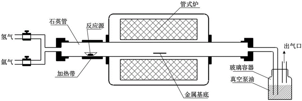
[0024] A method for preparing an atomic-level chalcogen compound film by chemical vapor deposition, comprising the following preparation steps:
[0025] (1) The molybdenum foil substrate with a thickness of 20 microns is first annealed at 1400 degrees for more than 10 hours in a hydrogen environment with a flow rate of 50sscm;
[0026] (2) Cut the annealed molybdenum foil into 3.5×2.5cm 2 The small piece is placed in a quartz tube furnace;
[0027] (3) Weigh 0.5 gram of sulfur powder, put it into the front end of the quartz tube, where it is heated with a heating tape;
[0028] (4) Seal the two ends of the quartz tube and vacuumize for 20 minutes to get rid of the remaining oxygen in the pipeline;
[0029] (5) After connecting one end of the quartz tube with the silicone tube, seal it with vacuum pump oil;
[0030] (6) Open the valve of the argon cylinder, inject argon into the quartz tube, and make its flow rate be 10 sccm;
[0031] (7) Turn on the tube furnace temperatur...
Embodiment 2
[0039] A method for preparing an atomic-level chalcogen compound film by chemical vapor deposition, comprising the following preparation steps:
[0040] (1) The molybdenum foil substrate with a thickness of 20 microns is first annealed at 1400 degrees for more than 10 hours in a hydrogen environment with a flow rate of 50sscm;
[0041] (2) Cut the annealed molybdenum foil into 3.5×2.5cm 2 The small piece is placed in a quartz tube furnace;
[0042] (3) Weigh 0.5 gram of sulfur powder, put it into the front end of the quartz tube, where it is heated with a heating tape;
[0043] (4) Seal the two ends of the quartz tube and vacuumize for 20 minutes to get rid of the remaining oxygen in the pipeline;
[0044] (5) After connecting one end of the quartz tube to the silicone tube, seal it with vacuum pump oil;
[0045] (6) Open the valve of the argon cylinder, inject argon into the quartz tube, and make its flow rate be 10 sccm;
[0046] (7) Turn on the tube furnace temperature ...
Embodiment 3
[0054] A method for preparing an atomic-level chalcogen compound film by chemical vapor deposition, comprising the following preparation steps:
[0055] (1) The molybdenum foil substrate with a thickness of 20 microns is first annealed at 1400 degrees for more than 10 hours in a hydrogen environment with a flow rate of 50sscm;
[0056] (2) Cut the annealed molybdenum foil into 3.5×2.5cm 2 The small piece is placed in a quartz tube furnace;
[0057] (3) Weigh 0.5 gram of selenium powder, put into the front end of quartz tube, use heating band to heat in this place;
[0058] (4) Seal the two ends of the quartz tube and vacuumize for 20 minutes to get rid of the remaining oxygen in the pipeline;
[0059] (5) After connecting one end of the quartz tube with the silicone tube, seal it with vacuum pump oil;
[0060] (6) open hydrogen and argon bottle valve, inject hydrogen and argon in quartz tube, make its flow rate be 2sccm and 18sccm;
[0061] (7) Turn on the tube furnace tem...
PUM
 Abstract
Description
Claims
Application Information
 - R&D
- Intellectual Property
- Life Sciences
- Materials
- Tech Scout
- Unparalleled Data Quality
- Higher Quality Content
- 60% Fewer Hallucinations
Browse by: Latest US Patents, China's latest patents, Technical Efficacy Thesaurus, Application Domain, Technology Topic, Popular Technical Reports.
© 2025 PatSnap. All rights reserved.Legal|Privacy policy|Modern Slavery Act Transparency Statement|Sitemap|About US| Contact US: help@patsnap.com


