Method for preparing titanium/diamond-like nanometer multilayer film on silicon surface
A diamond thin film and nano-multilayer technology, which is applied in the field of silicon surface modification, can solve the problems of low bonding strength of the diamond-like film film base, limited application and promotion, and peeling off, achieving high hardness, reducing surface friction and wear, and low interfacial stress Effect
- Summary
- Abstract
- Description
- Claims
- Application Information
AI Technical Summary
Problems solved by technology
Method used
Image
Examples
Embodiment 1
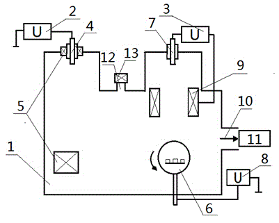
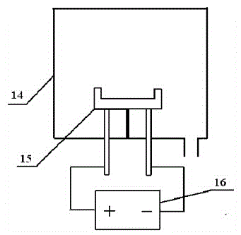
[0046] use figure 1 , figure 2 The shown device prepares a titanium / diamond-like nanometer multilayer film on the surface of a silicon substrate.
[0047] A single crystal silicon substrate with a diameter of 20 mm and a thickness of 0.5 mm is tested, and the operation steps are as follows:
[0048] (1) Silicon substrate surface treatment: put the monocrystalline silicon wafer into acetone solution, ethanol solution and deionized water for 10 minutes, respectively, to remove grease and other pollutants on the surface, and then place the substrate in an oven to dry for use;
[0049] (2) Fix the pretreated silicon substrate on such as figure 1 On the rotating sample stage 6 in the vacuum chamber 1 of the cathodic arc device shown, the high-purity titanium target 4 and the graphite target 7 are respectively installed on the evaporators of the DC cathodic arc 2 and the pulsed cathodic arc 3;
[0050] (3) Vacuumize the vacuum chamber 1 with a vacuum pumping device 11 to make ...
Embodiment 2
[0055] use figure 1 , figure 2 The shown device prepares a titanium / diamond-like nanometer multilayer film on the surface of a silicon substrate.
[0056] A single crystal silicon substrate with a diameter of 20 mm and a thickness of 0.5 mm is tested, and the operation steps are as follows:
[0057] (1) Silicon substrate surface treatment: put the monocrystalline silicon wafer into acetone solution, ethanol solution and deionized water for 10 minutes, respectively, to remove grease and other pollutants on the surface, and then place the substrate in an oven to dry for use;
[0058] (2) Fix the pretreated silicon substrate on such as figure 1 On the rotating sample stage 6 in the vacuum chamber 1 of the cathodic arc device shown, the high-purity titanium target 4 and the graphite target 7 are respectively installed on the evaporators of the DC cathodic arc 2 and the pulsed cathodic arc 3;
[0059] (3) Vacuumize the vacuum chamber 1 with a vacuum pumping device 11 to make ...
PUM
| Property | Measurement | Unit |
|---|---|---|
| thickness | aaaaa | aaaaa |
| friction coefficient | aaaaa | aaaaa |
| friction coefficient | aaaaa | aaaaa |
Abstract
Description
Claims
Application Information
 - R&D
- Intellectual Property
- Life Sciences
- Materials
- Tech Scout
- Unparalleled Data Quality
- Higher Quality Content
- 60% Fewer Hallucinations
Browse by: Latest US Patents, China's latest patents, Technical Efficacy Thesaurus, Application Domain, Technology Topic, Popular Technical Reports.
© 2025 PatSnap. All rights reserved.Legal|Privacy policy|Modern Slavery Act Transparency Statement|Sitemap|About US| Contact US: help@patsnap.com


