Transparent laminated film, transparent conductive film, and gas barrier laminated film
A transparent conductive film and transparent conductive layer technology, applied to the conductive layer on the insulating carrier, electrical components, non-metallic conductors, etc., can solve the problems of surface resistance, poor durability and acid resistance, etc., to improve crystallinity, reduce Effect of surface resistance value
- Summary
- Abstract
- Description
- Claims
- Application Information
AI Technical Summary
Problems solved by technology
Method used
Image


Examples
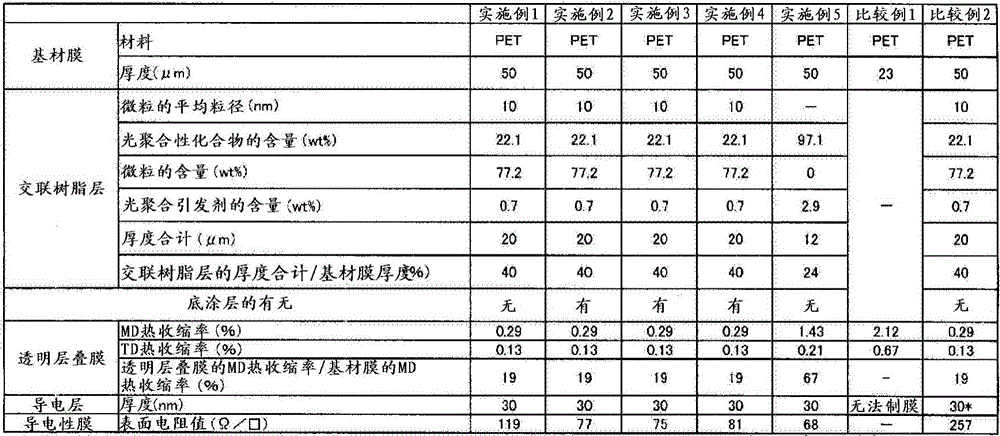
Embodiment 1
[0301] (Preparation of Photocurable Composition 1)
[0302] 22.1% by mass of a photocurable bifunctional acrylate monomer (tricyclodecane dimethanol diacrylate, molecular weight 304, manufactured by Shin-Nakamura Chemical Industry Co., Ltd., trade name "A-DCP"), silica microparticles (Co., Ltd. Admatechs Co., Ltd., trade name "YA010C-SM1", average particle diameter 10nm) 77.2% by mass, photopolymerization initiator A (manufactured by BASF, trade name "IRGACURE127") 0.6 mass%, photopolymerization initiator B (manufactured by BASF, commercial product Name "IRGACURE184") 0.1% by mass was uniformly diluted with a solvent (propylene glycol monomethyl ether) to obtain a curable composition 1 (coating A) for forming a crosslinked resin layer.
[0303] (Production of transparent laminated film 1)
[0304] On one side of a biaxially stretched polyethylene terephthalate film (manufactured by Mitsubishi Plastics Corporation, trade name "Diafoil") with a thickness of 50 μm using a die co...
Embodiment 2
[0310] (Production of transparent laminated film 2)
[0311] On one side of the transparent laminated film 1 produced in Example 1, 88% by mass of a polyester resin (PESRESIN A-215GE manufactured by Takamatsu Yushishishishishishishishi Co., Ltd.) containing 12% by mass of an oxazoline-based polymer (EPOCROS WS-700 manufactured by Nippon Shokubai Co., Ltd.) was uniformly diluted with water to obtain a transparent laminated film in which a primer layer was formed on one side of the crosslinked resin layer of the transparent laminated film 1 2.
[0312] (Fabrication of Transparent Conductive Film 2 Formed with Transparent Conductive Layer)
[0313]An ITO film was formed as a transparent conductive layer with a thickness of 30 nm on the undercoat layer surface of the transparent multilayer film 2 by a sputtering method in a 200° C. environment. When the surface resistance value of the conductive layer of the obtained transparent conductive film 2 was measured with Loresta EP (m...
Embodiment 3
[0315] (Production of transparent laminated film 3)
[0316] One side of the transparent laminated film 1 produced in Example 1 was coated with a hard coat paint (NK hard B500 manufactured by Shin Nakamura Chemical Industry Co., Ltd.) so that the thickness after drying became 3 μm, and it was further cured using an ultraviolet irradiation device. Thus, the transparent laminated film 3 in which the undercoat layer was formed on one side of the crosslinked resin layer of the transparent laminated film 1 was obtained.
[0317] (Fabrication of Transparent Conductive Film 3 Formed with Transparent Conductive Layer)
[0318] An ITO film was formed as a transparent conductive layer with a thickness of 30 nm on the undercoat surface of the transparent multilayer film 3 by a sputtering method in a 200° C. environment. When the surface resistance value of the conductive layer of the obtained transparent conductive film 3 was measured with Loresta EP (manufactured by Mitsubishi Chemical...
PUM
| Property | Measurement | Unit |
|---|---|---|
| thickness | aaaaa | aaaaa |
| particle size | aaaaa | aaaaa |
| glass transition temperature | aaaaa | aaaaa |
Abstract
Description
Claims
Application Information
 - Generate Ideas
- Intellectual Property
- Life Sciences
- Materials
- Tech Scout
- Unparalleled Data Quality
- Higher Quality Content
- 60% Fewer Hallucinations
Browse by: Latest US Patents, China's latest patents, Technical Efficacy Thesaurus, Application Domain, Technology Topic, Popular Technical Reports.
© 2025 PatSnap. All rights reserved.Legal|Privacy policy|Modern Slavery Act Transparency Statement|Sitemap|About US| Contact US: help@patsnap.com