
In-cell liquid crystal panel and liquid crystal display device

A liquid crystal panel and liquid crystal layer technology, applied in optics, instruments, electrical and digital data processing, etc., can solve the problems of unstable sensor electrode capacity, reduced sensitivity of touch panel, disturbance of electric field, etc., achieve good antistatic function, inhibit conduction Defects, the effect of reducing the surface resistance value

Pending Publication Date: 2019-11-15
NITTO DENKO CORP
View PDF15 Cites 0 Cited by
  • Summary
  • Abstract
  • Description
  • Claims
  • Application Information

AI Technical Summary

Problems solved by technology

When there is a conductive layer such as an antistatic layer between the above-mentioned transparent electrode pattern and the user's finger, the electric field between the drive electrode and the sensor electrode is disturbed, the capacitance of the sensor electrode becomes unstable, the sensitivity of the touch panel decreases, and malfunction occurs. s reason

Method used

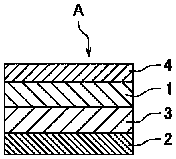
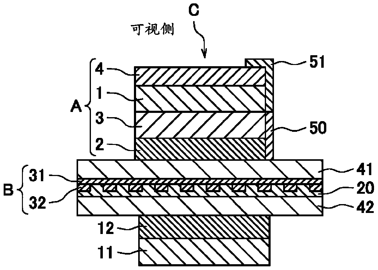
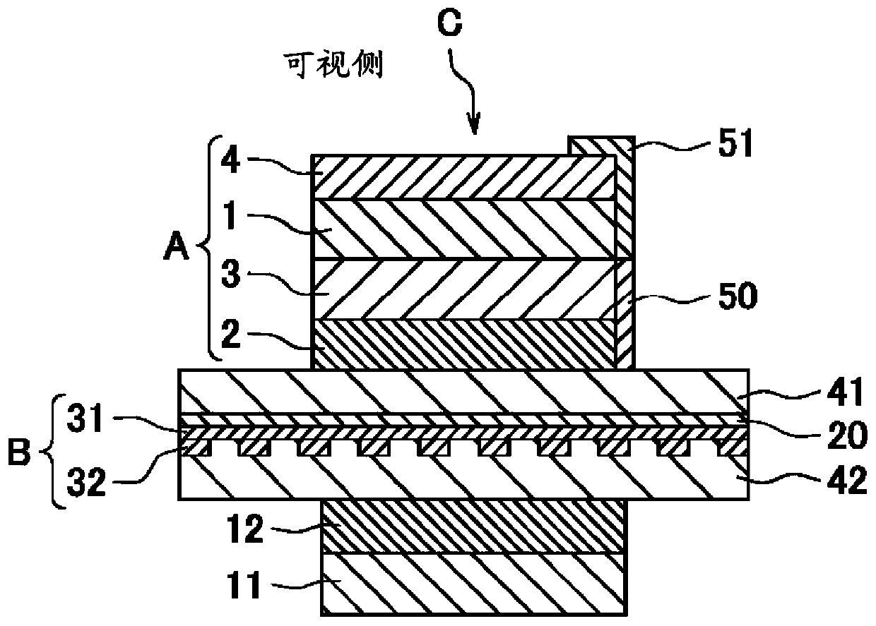

Image

  • In-cell liquid crystal panel and liquid crystal display device
  • In-cell liquid crystal panel and liquid crystal display device
  • In-cell liquid crystal panel and liquid crystal display device

Examples


Embodiment 1~12 and comparative example 1~3

[0173] An adhesive layer was sequentially formed on one side of the polarizing film obtained above (the side not provided with the surface treatment layer described in Table 1) in the combinations shown in Table 1 to prepare a polarizing film with an adhesive layer.

[0174] In addition, in Comparative Examples 1 and 2, no surface treatment layer (hard coat layer) was formed. In addition, in Examples 1, 2, and Comparative Example 1, no ionic compound was blended when preparing the adhesive composition.

[0175] The following evaluations were performed about the polarizing film with an adhesive layer obtained in the said Example and the comparative example. Table 1 shows the evaluation results.

[0176]

[0177] Surface resistance values ​​were measured for the surface treatment layer and the pressure-sensitive adhesive layer.

[0178] The surface resistance value of the surface treatment layer was measured about the surface treatment layer of the polarizing film with an adhe...


PUM

PropertyMeasurementUnit
thicknessaaaaaaaaaa
particle sizeaaaaaaaaaa
thicknessaaaaaaaaaa

Abstract

The present invention provides an in-cell liquid crystal panel having: an in-cell liquid crystal cell that is provided with a liquid crystal layer comprising liquid crystal molecules which are homogeneously oriented when no electric field is present, a first transparent substrate and a second transparent substrate sandwiching the liquid crystal layer on both sides, and a touch sensing electrode portion related to touch sensor and touch-driven functions between the first transparent substrate and the second transparent substrate; and a polarizing film with added adhesive layer that is disposed,via a first adhesive layer and without interposing a conductive layer, to the first transparent substrate side on the viewing side of the in-cell liquid crystal cell. The polarizing film with added adhesive layer is provided with a surface treatment layer, a first polarizing film, and the first adhesive layer in this order. The surface treatment layer includes at least one of any antistatic agentselected from ionic surfactants, conductive microparticles, and conductive polymers. In the in-cell liquid crystal panel, the antistatic function is satisfactory and it is possible to satisfy touch sensor sensitivity as well as conduction reliability and durability in humid environments.

Description

technical field [0001] The present invention relates to an in-cell type liquid crystal cell having a touch sensor function introduced inside the liquid crystal cell, and an in-cell type liquid crystal cell having a polarizing film with an adhesive layer on the visible side of the in-cell type liquid crystal cell LCD panel. In addition, the present invention also relates to a liquid crystal display device using the liquid crystal panel. The liquid crystal display device with a touch sensor function using an in-cell liquid crystal panel of the present invention can be used as various input display devices such as mobile devices. Background technique [0002] A liquid crystal display device usually has a polarizing film bonded from both sides of the liquid crystal cell through an adhesive layer according to its image forming method. In addition, products in which a touch panel is mounted on a display screen of a liquid crystal display device are also put into practical use. ...

Claims


Application Information

Patent Timeline
Patent Type & Authority Applications(China)
IPC IPC(8): G02F1/1333G02B1/14G02B1/16G02B5/30G02F1/1335G06F3/041G06F3/044
CPCG02B1/14G02B1/16G06F3/0446G06F3/0445G06F3/0412G06F2203/04105G02B1/11G02B5/3033G02F2202/22G02F1/133528G02F1/1333G06F3/041G02F1/1335G02B5/30G02F1/133738G02F1/13338G02F1/134309G02F2201/50G02F2202/28
Inventor 藤田昌邦外山雄祐
Owner NITTO DENKO CORP
Learn More