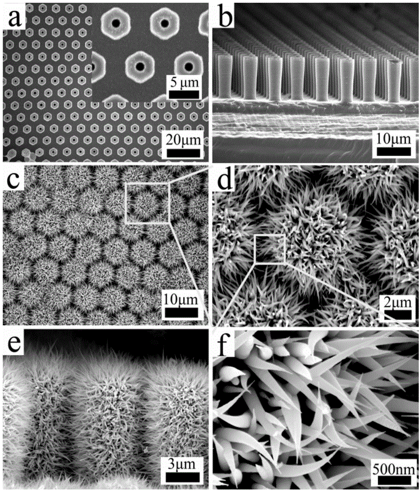
Silver-germanium-silicon heterogeneous hierarchical structure array, and preparation method and application of array
A hierarchical structure and array technology, applied in the direction of material excitation analysis, nanotechnology for materials and surface science, gaseous chemical plating, etc., can solve the problems of unfavorable adsorption of substances to be detected, small surface area, and few precious metal nanoparticles. Achieve the effects of good consistency and repeatability of detection, scientific preparation method and reasonable structure
- Summary
- Abstract
- Description
- Claims
- Application Information
AI Technical Summary
Problems solved by technology
Method used
Image
Examples
Embodiment 1
[0036] The specific steps of preparation are:
[0037] In step 1, firstly mix 81 g / L of nickel nitrate solution and 2.2 g / L of graphene oxide solution in a ratio of 1:1 by volume to obtain a mixed solution. Then, the hexagonal silicon micron hexagonal prism array obtained by using photolithography and deep silicon etching technology is immersed in the mixed solution for 25 minutes to obtain a hexagonal silicon micron hexagonal prism array whose surface is modified with nickel nitrate.
[0038] Step 2: After placing the hexagonal silicon micron hexagonal prism array modified with nickel nitrate on the surface of the chemical vapor deposition furnace cavity, the chemical vapor deposition furnace cavity and gas path are sequentially vacuumed and cleaned with argon. Subsequently, the furnace cavity was first placed under an argon atmosphere, and the temperature was increased from room temperature to 290°C at a temperature increase rate of 10°C / min. Then the furnace chamber was kept in...
Embodiment 2
[0040] The specific steps of preparation are:
[0041] In step 1, first, 86 g / L of nickel nitrate solution and 2.1 g / L of graphene oxide solution are mixed in a ratio of 1:1 by volume to obtain a mixed solution. Then, the hexagonal silicon micron hexagonal prism array obtained by using photolithography and deep silicon etching technology was immersed in the mixed solution for 26 minutes to obtain a hexagonal silicon micron hexagonal prism array whose surface was modified with nickel nitrate.
[0042] Step 2: After placing the hexagonal silicon micron hexagonal prism array modified with nickel nitrate on the surface of the chemical vapor deposition furnace cavity, the chemical vapor deposition furnace cavity and gas path are sequentially vacuumed and cleaned with argon. Subsequently, the furnace cavity was first placed under an argon atmosphere, and the temperature was increased from room temperature to 300°C at a temperature increase rate of 10°C / min. Then the furnace chamber was ...
Embodiment 3
[0044] The specific steps of preparation are:
[0045] Step 1. First, mix 91 g / L of nickel nitrate solution and 2 g / L of graphene oxide solution in a ratio of 1:1 by volume to obtain a mixed solution. Then, the hexagonal silicon micron hexagonal prism array obtained by using photolithography and deep silicon etching technology was immersed in the mixed solution for 27 minutes to obtain a hexagonal silicon micron hexagonal prism array whose surface was modified with nickel nitrate.
[0046] Step 2: After placing the hexagonal silicon micron hexagonal prism array modified with nickel nitrate on the surface of the chemical vapor deposition furnace cavity, the chemical vapor deposition furnace cavity and gas path are sequentially vacuumed and cleaned with argon. Subsequently, the furnace cavity was first placed under an argon atmosphere, and the temperature was increased from room temperature to 310°C at a temperature increase rate of 10°C / min. Then the furnace chamber was kept in a d...
PUM
| Property | Measurement | Unit |
|---|---|---|
| diameter | aaaaa | aaaaa |
| particle diameter | aaaaa | aaaaa |
| height | aaaaa | aaaaa |
Abstract
Description
Claims
Application Information
 - Generate Ideas
- Intellectual Property
- Life Sciences
- Materials
- Tech Scout
- Unparalleled Data Quality
- Higher Quality Content
- 60% Fewer Hallucinations
Browse by: Latest US Patents, China's latest patents, Technical Efficacy Thesaurus, Application Domain, Technology Topic, Popular Technical Reports.
© 2025 PatSnap. All rights reserved.Legal|Privacy policy|Modern Slavery Act Transparency Statement|Sitemap|About US| Contact US: help@patsnap.com


