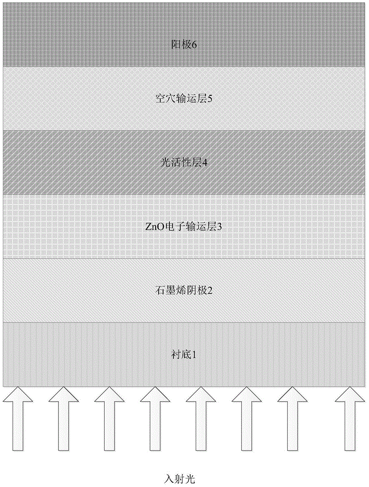
Planar perovskite solar cell based on graphene ZnO cathode and preparation method thereof
A technology of solar cells and graphene, applied in circuits, photovoltaic power generation, electrical components, etc., can solve the problems of not being suitable for preparing large-area thin films, being incompatible with flexible substrates, and high cost, so as to improve energy conversion efficiency and environmental protection Quality, low cost effect
- Summary
- Abstract
- Description
- Claims
- Application Information
AI Technical Summary
Problems solved by technology
Method used
Image
Examples
Embodiment 1
[0030] Example 1: Fabrication of a solar cell with a thickness of 70 nm of ZnO electron transport layer.
[0031] Step 1, cleaning the substrate substrate.
[0032] The graphene glass substrate with a thickness of 20 nm was sequentially placed in deionized water, acetone, absolute ethanol and deionized water for ultrasonic cleaning for 5 minutes, and dried with a nitrogen gun after cleaning.
[0033] Step 2, deposit a ZnO electron transport layer.
[0034] 2a) Configure ZnO precursor solution: Dissolve 150mg of ZnO powder with particle size less than 5um in 15ml ammonia with a concentration of 25%, and put it in the refrigerator after 5min ultrasonic vibration, at a refrigeration temperature of 5℃, and a refrigeration time of 24h to obtain ZnO precursor solution with a concentration of 0.125M / L;
[0035] 2b) Spin-coating the ZnO precursor solution on the graphene at a spin-coating speed of 4000r / min, a spin-coating time of 40s, and annealing in an oven at a temperature of 100°C for 5mi...
Embodiment 2
[0047] Example 2: Fabrication of a solar cell with a thickness of 70 nm of the ZnO electron transport layer.
[0048] Step one, clean the substrate substrate
[0049] The graphene glass substrate covered with a thickness of 25nm was sequentially placed in deionized water, acetone, absolute ethanol and deionized water for ultrasonic cleaning for 10 minutes, and then dried with a nitrogen gun after cleaning.
[0050] Step two, deposit a ZnO electron transport layer.
[0051] 2. A) The specific implementation of this step is the same as step 2a) of embodiment 1;
[0052] 2. Two) Spin-coating the ZnO precursor solution on the graphene with a spin-coating speed of 3000 r / min and a spin-coating time of 40 s, and annealing in an oven at a temperature of 150° C. for 10 minutes, the obtained ZnO thickness is 85 nm. Step three, spin-coating PbI 2 Solution.
[0053] First, 460mg of PbI 2 Dissolve in 1ml of dimethylacetamide DMF and stir at 90℃ for 6h to obtain 460 / mL clear PbI 2 Solution
[0054] T...
Embodiment 3
[0064] Example 3: Manufacturing a solar cell with a thickness of 100 nm of the ZnO electron transport layer.
[0065] Step A, cleaning the substrate substrate.
[0066] The graphene glass substrate covered with a thickness of 40 nm was sequentially placed in deionized water, acetone, absolute ethanol and deionized water for ultrasonic cleaning for 15 minutes, and dried with a nitrogen gun after cleaning.
[0067] Step B, deposit a ZnO electron transport layer.
[0068] B1) The specific implementation of this step is the same as step 2a) of embodiment 1;
[0069] B2) Spin-coating the ZnO precursor solution on the graphene at a spin-coating speed of 2000r / min and a spin-coating time of 40s, and annealed in an oven at a temperature of 200°C for 10 minutes, to obtain a ZnO thickness of 100nm.
[0070] Step C, spin coating PbI 2 Solution.
[0071] 460mg of PbI 2 Dissolve in 1ml of dimethylacetamide DMF and stir at 90℃ for 6h to obtain 460 / mL clear PbI 2 Solution; then spin-coated PbI on the su...
PUM
 Abstract
Description
Claims
Application Information
 - R&D Engineer
- R&D Manager
- IP Professional
- Industry Leading Data Capabilities
- Powerful AI technology
- Patent DNA Extraction
Browse by: Latest US Patents, China's latest patents, Technical Efficacy Thesaurus, Application Domain, Technology Topic, Popular Technical Reports.
© 2024 PatSnap. All rights reserved.Legal|Privacy policy|Modern Slavery Act Transparency Statement|Sitemap|About US| Contact US: help@patsnap.com


