
High-power laser for 808nm ceiling light field

A technology of high-power lasers and flat top light, which is applied to lasers, laser components, semiconductor lasers, etc., can solve problems such as high working voltage, low electro-optical conversion efficiency, and change the reliability of lasers, so as to reduce voltage drop and improve Optical damage threshold, effect of increasing near-field spot size

Active Publication Date: 2015-05-06
THE 13TH RES INST OF CHINA ELECTRONICS TECH GRP CORP
View PDF5 Cites 2 Cited by
  • Summary
  • Abstract
  • Description
  • Claims
  • Application Information

AI Technical Summary

Problems solved by technology

However, the fast axis optical field is concentrated in the active area, and the optical power density in the active area is still high, which does not substantially change the reliability of the laser.
At the same time, there are defects such as high working voltage and low electro-optical conversion efficiency.

Method used

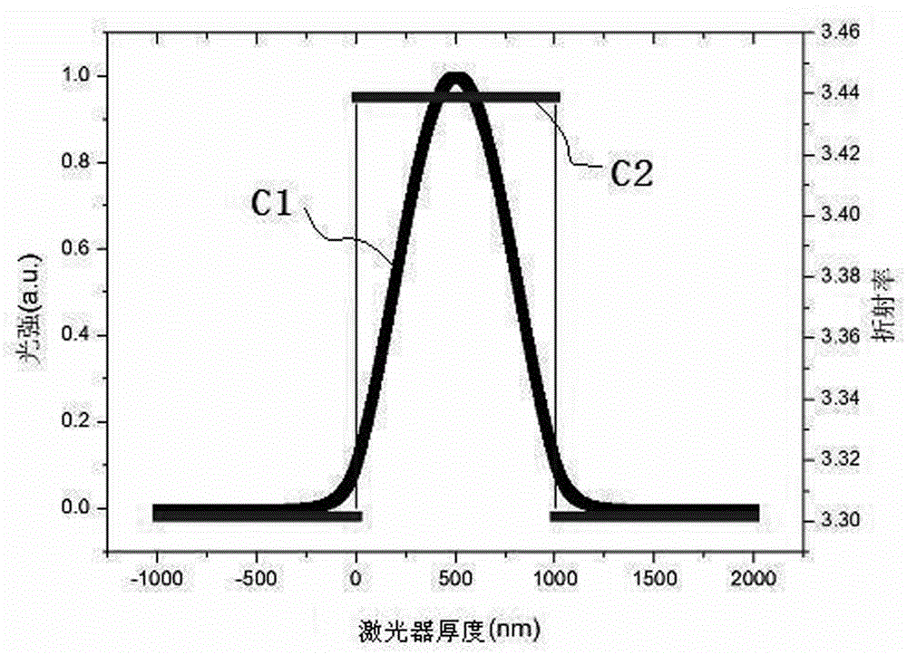
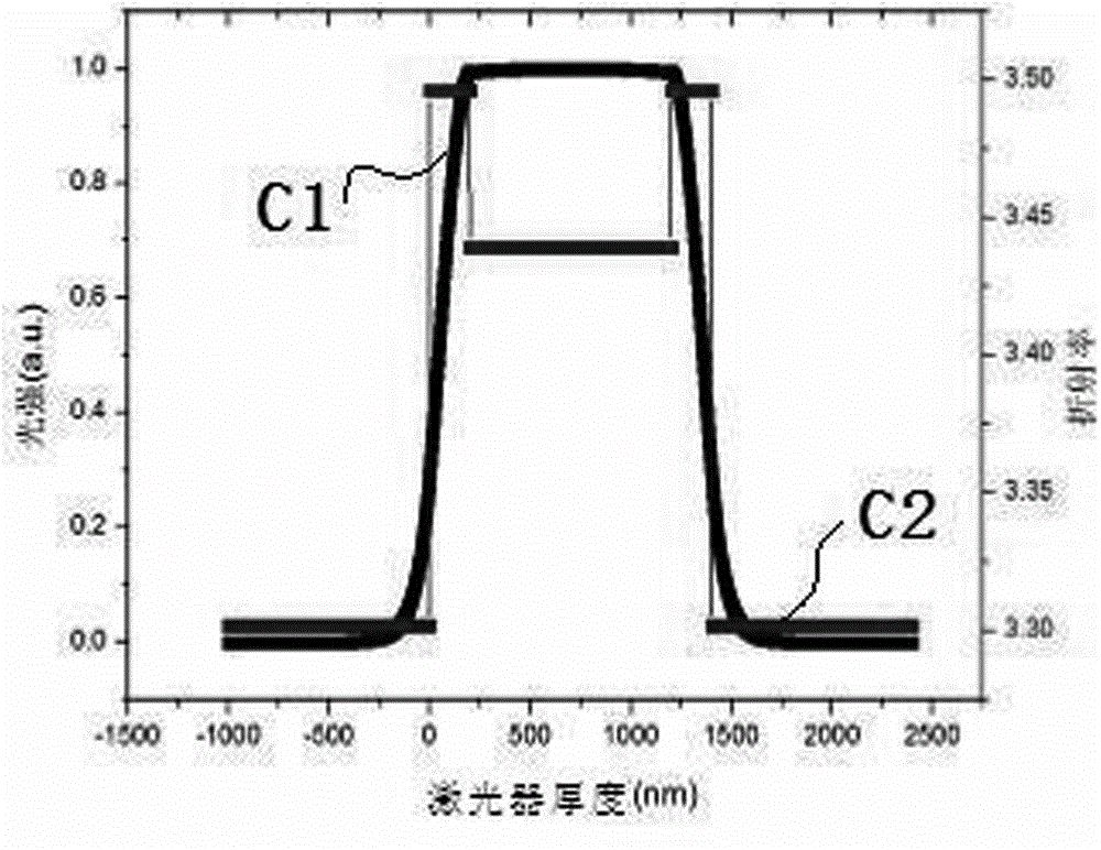

Image

  • High-power laser for 808nm ceiling light field
  • High-power laser for 808nm ceiling light field
  • High-power laser for 808nm ceiling light field

Examples


Embodiment 1

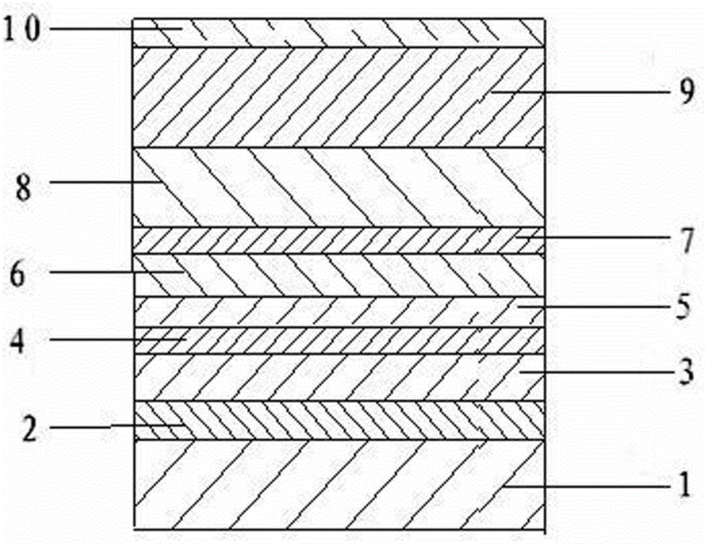
[0021] Such as figure 1 As shown, the 808nm flat-top optical field high-power laser includes a substrate 1, a buffer layer 2, a lower confinement layer 3, a lower optical field effect layer 4, a lower waveguide layer 5, a quantum well layer 6, an upper waveguide layer 7, and an upper optical layer. Field effect layer 8 , upper confinement layer 9 and electrode contact layer 10 .

[0022] The substrate 1 is used for the epitaxial growth of each layer of semiconductor laser materials. In the present invention, the substrate 1 is N-type gallium arsenide on the (100) plane, which can facilitate the injection of electrons and reduce the material of the substrate 1. of series resistance.

[0023] The buffer layer 2 is fabricated on the substrate 1 and is an N-type gallium arsenide material. Its purpose is to form a high-quality epitaxial surface, reduce the stress on the substrate 1 and other layers, and eliminate the defects of the substrate 1 to other layers. Propagation, in ord...


PUM

PropertyMeasurementUnit
Thicknessaaaaaaaaaa
Thicknessaaaaaaaaaa
Doping concentrationaaaaaaaaaa

Abstract

The invention discloses a high-power laser for a 808nm ceiling light field and relates to the technical field of a semiconductor laser; the high-power laser comprises a substrate, wherein a buffer layer, a lower limiting layer, a lower light-field active layer, a lower waveguide layer, a quantum well layer, an upper waveguide layer, an upper light-field active layer, an upper limiting layer and an electrode contact layer are sequentially grown on the substrate from top to bottom; the lower light-field active layer is made of a highly doped N-type AlGaAs material, and the upper light-field active layer is made of a highly doped P-type AlGaAs material. The light field top of the fast axis is uniformly distributed, so that the optical power density in the active region can be further reduced, and reliability and durability of the laser are improved.

Description

technical field [0001] The invention relates to the technical field of semiconductor lasers. Background technique [0002] 808nm high-power semiconductor lasers have been more and more widely used in the fields of solid-state laser pumping, laser processing, laser medical treatment, laser display and military applications, especially in solid-state laser pumping applications, because of their small size and light weight , high efficiency and reliability are favored. In the past ten years, with the further maturity of high-power semiconductor laser products, the output power of linear arrays and stacked array modules packaged into laser bars through various structures can reach thousands of watts or even tens of thousands of watts. The demand in the field has grown considerably. [0003] For high-power semiconductor lasers, the semiconductor material on the cavity surface is prone to damage under high optical power density, thereby destroying the reflection or transmission ...

Claims


Application Information

Patent Timeline
IPC IPC(8): H01S5/323H01S5/20
Inventor 宁吉丰陈宏泰车相辉王彦照林琳位永平王晶
Owner THE 13TH RES INST OF CHINA ELECTRONICS TECH GRP CORP
Learn More