Research method on microstructure evolution in SiO2 thin film growth process
A technology of microstructure evolution and thin film growth, applied in the field of reverse research, can solve the problems of cost and long research cycle
- Summary
- Abstract
- Description
- Claims
- Application Information
AI Technical Summary
Problems solved by technology
Method used
Image
Examples
Embodiment
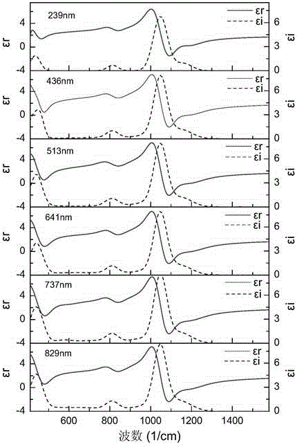
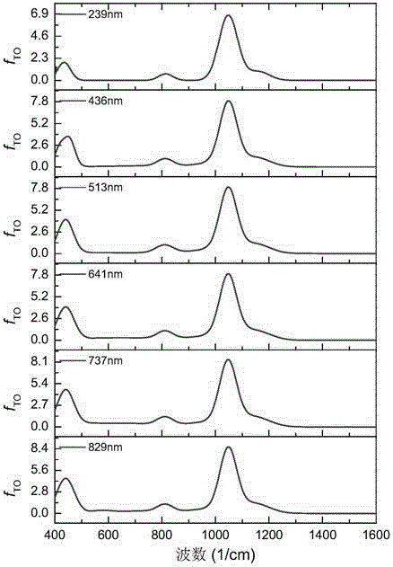
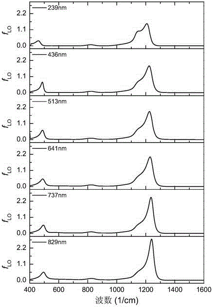
[0060] SiO prepared by ion beam sputtering in this example 2 Taking a thin film as an example, the above method is used to evaluate the evolution law of the Si-O-Si bond angle during the growth process, and to determine the development trend of its short-range order structure.
[0061] 1) The thin film sample substrate uses an ultra-smooth Si sheet (surface roughness ~0.3nm, Φ40×0.32mm), and SiO is prepared by ion beam sputtering deposition method. 2 film. The specific process parameters are as follows: ion beam sputtering deposition using SiO 2 Target material (purity ≥ 99.99%), background vacuum degree is better than 1.0×10⁻³Pa, substrate temperature is room temperature, ion beam voltage is 1250V, ion beam current is 500mA, oxygen flow rate is 30sccm, deposition time is 3600s, thin film physics The thickness is about 850nm.
[0062] 2) The method of chemical corrosion on SiO 2 Thin film layered corrosion, using hydrofluoric acid + ammonia water + glycerol + ethylene glyc...
PUM
 Abstract
Description
Claims
Application Information
 - R&D
- Intellectual Property
- Life Sciences
- Materials
- Tech Scout
- Unparalleled Data Quality
- Higher Quality Content
- 60% Fewer Hallucinations
Browse by: Latest US Patents, China's latest patents, Technical Efficacy Thesaurus, Application Domain, Technology Topic, Popular Technical Reports.
© 2025 PatSnap. All rights reserved.Legal|Privacy policy|Modern Slavery Act Transparency Statement|Sitemap|About US| Contact US: help@patsnap.com


