Method for forming nmos metal gate transistors
A metal gate and transistor technology, applied in semiconductor devices, semiconductor/solid-state device manufacturing, electrical components, etc., can solve problems such as poor performance of TDDB, achieve the effect of reducing the number of dangling bonds, improving the surface state, and improving the performance of TDDB
- Summary
- Abstract
- Description
- Claims
- Application Information
AI Technical Summary
Problems solved by technology
Method used
Image

Examples
no. 1 example
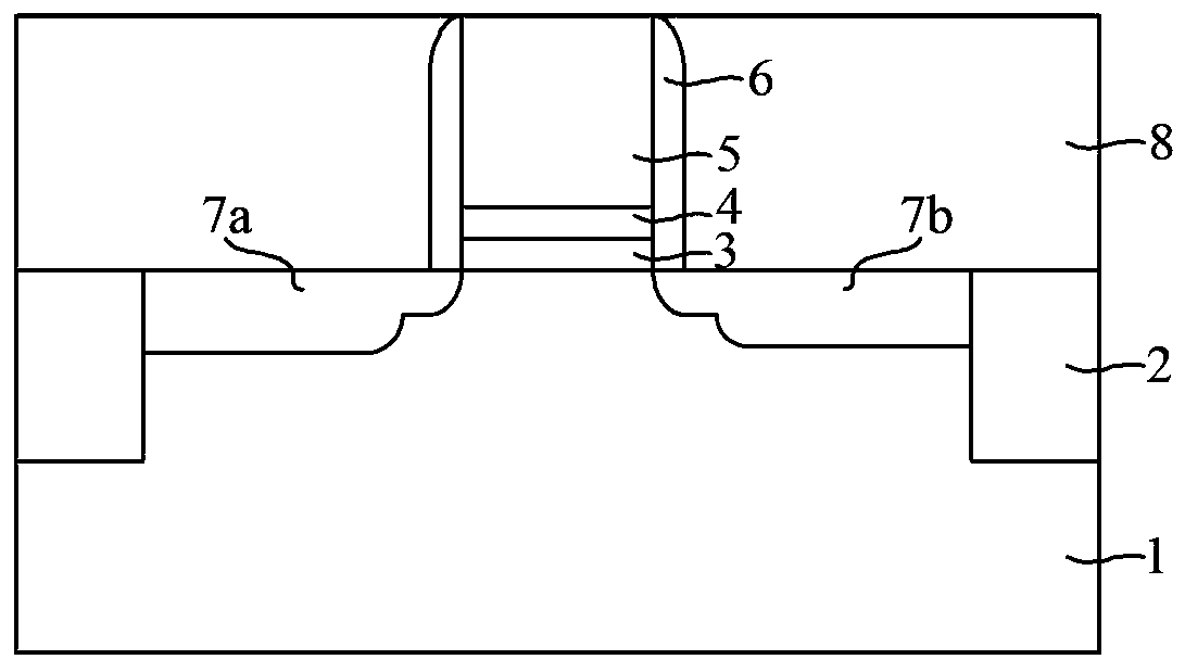
[0047] First, if Figure 4 As shown, a substrate 100 is provided.
[0048]The substrate 100 may be a common substrate such as a silicon substrate, a silicon germanium substrate, gallium arsenic, and the like. In a specific embodiment, the substrate 100 has a P well 101 for forming an NMOS metal gate transistor at a position corresponding to the P well 101; in addition, the substrate 100 also has a shallow trench isolation structure 102 for forming the NMOS Metal gate transistors are electrically isolated from other devices on the same substrate.
[0049] Continue to refer to Figure 4 As shown, a dummy gate structure is formed on a substrate 100, and the dummy gate structure includes: a gate dielectric layer 110, a nitrogen-containing diffusion barrier layer 120 located on the gate dielectric layer 110, and a dummy gate located on the nitrogen-containing diffusion barrier layer 120 Pole 130.
[0050] The gate dielectric layer 110 may be a high-k dielectric layer, or a stac...
no. 2 example
[0088] The difference between the second embodiment and the first embodiment is: after removing the dummy gate and before performing plasma treatment, only plasma etching is performed on the bottom of the trench with fluorine-containing plasma. In other words, in the second embodiment, only one plasma etch step is utilized to remove the polymer on the surface of the nitrogen-containing diffusion barrier layer.
[0089] In this embodiment, the fluorine-containing gas is plasmatized to generate the fluorine-containing plasma, and the fluorine-containing gas includes at least CF 4 、NF 3 , SF 6 One of.
[0090] Compared with the second embodiment in which only one plasma etching step is used to remove the polymer, since the first embodiment uses two plasma etching steps to remove the polymer, each plasma in the first embodiment The ion bombardment energy in the etching step can be smaller, which reduces the damage to the nitrogen-containing diffusion barrier layer, which is con...
no. 3 example
[0093] The difference between the third embodiment and the first embodiment is that in the step of removing the dummy gate, there is no metal hard mask layer between the silicon oxide layer and the photoresist layer.
[0094] In other words, in the third embodiment, the method for removing the dummy gate includes: forming a silicon oxide layer on the interlayer dielectric layer and the dummy gate, and a photoresist layer on the silicon oxide layer; The silicon oxide layer is patterned to form an opening in the photoresist layer and the silicon oxide layer, the opening corresponds to the position of the dummy gate, and the bottom of the opening exposes the dummy gate; the patterned photoresist layer and The patterned silicon oxide layer is used as a mask for dry etching to remove the dummy gate and form a trench at the position of the dummy gate; after removing the dummy gate, the photoresist layer is removed.
[0095] In the third embodiment, the function of disposing the sili...
PUM
| Property | Measurement | Unit |
|---|---|---|
| thickness | aaaaa | aaaaa |
Abstract
Description
Claims
Application Information
 - R&D
- Intellectual Property
- Life Sciences
- Materials
- Tech Scout
- Unparalleled Data Quality
- Higher Quality Content
- 60% Fewer Hallucinations
Browse by: Latest US Patents, China's latest patents, Technical Efficacy Thesaurus, Application Domain, Technology Topic, Popular Technical Reports.
© 2025 PatSnap. All rights reserved.Legal|Privacy policy|Modern Slavery Act Transparency Statement|Sitemap|About US| Contact US: help@patsnap.com