A kind of growth method of Aln epitaxial layer with high crystal quality
A growth method and technology of crystal quality, applied in semiconductor/solid-state device manufacturing, electrical components, circuits, etc., can solve the problems of uneven surface, high dislocation density of AlN epitaxial layers with high crystal quality, etc., and achieve low dislocation density, The method is simple and easy to implement, and the surface is smooth
- Summary
- Abstract
- Description
- Claims
- Application Information
AI Technical Summary
Problems solved by technology
Method used
Image

Examples
preparation example Construction
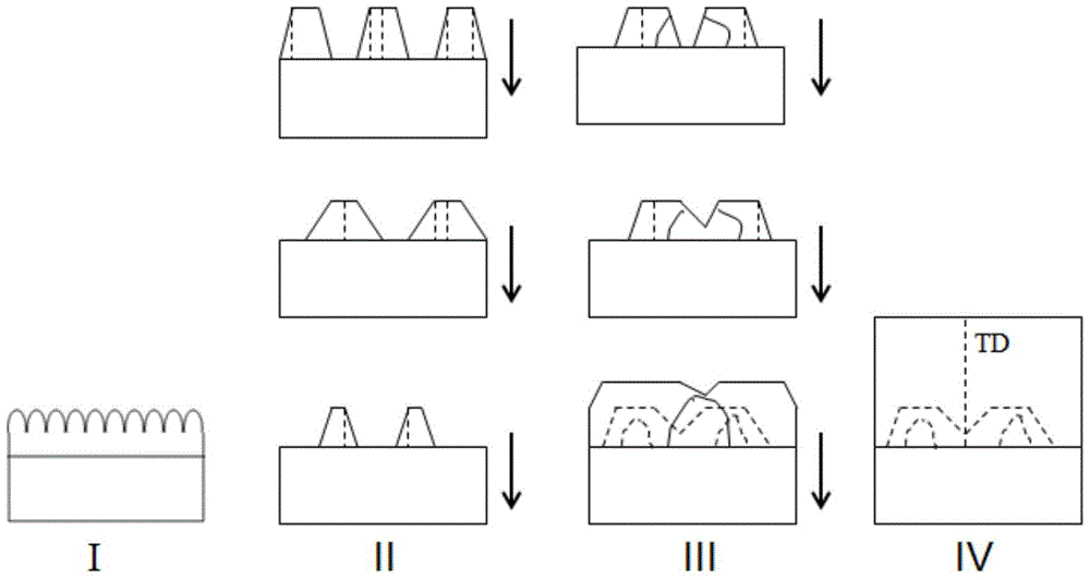
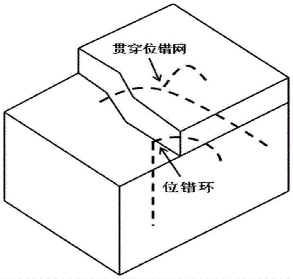
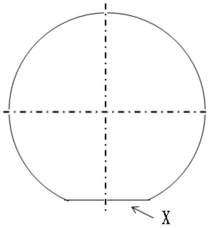
[0053] The preparation method of the present invention includes several stages such as substrate baking, substrate nitriding, low-temperature deposition of AlN nucleation layer, temperature rise, and high-temperature epitaxial growth of AlN. In order to grow the AlN epitaxial layer with high crystal quality, the technical points of the present invention have three points. One is the introduction of the substrate nitriding process, which modifies the surface of the sapphire substrate to change its microstructure, which is conducive to achieving extremely low screw dislocation density. The second is to use a sapphire substrate with a large inclination angle (choose C off M (or A) 1°-4°). Changing the inclination angle of the substrate can effectively cut the atomic step width of the substrate surface. For example, when the inclination angle changes from 2° to 4°, The step width can be reduced from 37.2nm to 18.6nm, which is far smaller than the step width 372.2nm of the widely u...
Embodiment 1
[0056] 1) Metal-organic chemical vapor deposition (MOCVD) equipment (3×2”Thomas Swan CCS MOCVD), the substrate is a sapphire substrate with C off M 2° (0001) plane, H2 is introduced, and the reaction chamber pressure is 120mbar , bake at 1100°C for 600s, and clean the substrate.
[0057] 2) Lower the temperature to 950°C, pass through ammonia gas for nitriding for 7s, H2 is used as carrier gas, and the pressure of the reaction chamber is 100mbar. And feed trimethylaluminum into the reaction chamber.
[0058] 3) Low-temperature AlN is grown at 950°C, and the growth thickness is 10nm.
[0059] 4) Keep the pressure of the reaction chamber at 100 mbar, stop feeding trimethylaluminum, continue feeding ammonia gas, raise the temperature to 1100° C. in 200 seconds, and stabilize for 20 seconds.
[0060] 5) Feed ammonia gas and trimethylaluminum, keep the reaction chamber pressure at 80 mbar, temperature at 1100° C., V / III molar ratio at 375, high temperature epitaxial growth of AlN...
Embodiment 2
[0065] 1) Metal-organic chemical vapor deposition (MOCVD) equipment (3×2”Aixtron CCS FP-MOCVD), the substrate is a sapphire substrate with C off M 4° (0001) plane, H2 is introduced, and the reaction chamber pressure is 120mbar, bake at 1100°C for 600s, and clean the substrate.
[0066] 2) Lower the temperature to 930° C., pass through ammonia gas for nitriding for 10 seconds, H2 is used as carrier gas, and the pressure of the reaction chamber is 90 mbar. And feed trimethylaluminum into the reaction chamber.
[0067] 3) Low-temperature AlN is grown at 930°C, and the growth thickness is 10nm.
[0068] 4) Keep the pressure of the reaction chamber at 100 mbar, stop feeding trimethylaluminum, continue feeding ammonia gas, raise the temperature to 1000° C. in 100 seconds, and stabilize for 20 seconds.
[0069] 5) Feed ammonia gas and trimethylaluminum, keep the reaction chamber pressure at 60mbar, temperature at 1000°C, V / III molar ratio at 200, high temperature epitaxial growth o...
PUM
| Property | Measurement | Unit |
|---|---|---|
| thickness | aaaaa | aaaaa |
Abstract
Description
Claims
Application Information
 - R&D
- Intellectual Property
- Life Sciences
- Materials
- Tech Scout
- Unparalleled Data Quality
- Higher Quality Content
- 60% Fewer Hallucinations
Browse by: Latest US Patents, China's latest patents, Technical Efficacy Thesaurus, Application Domain, Technology Topic, Popular Technical Reports.
© 2025 PatSnap. All rights reserved.Legal|Privacy policy|Modern Slavery Act Transparency Statement|Sitemap|About US| Contact US: help@patsnap.com