
AIN film preparing method

A technology of thin film and epitaxial thin film, which is applied in the field of preparation of AlN thin film, can solve the problems of low dislocation density AlN thin film, etc.

Active Publication Date: 2011-08-17
常熟紫金知识产权服务有限公司
View PDF0 Cites 0 Cited by
  • Summary
  • Abstract
  • Description
  • Claims
  • Application Information

AI Technical Summary

Problems solved by technology

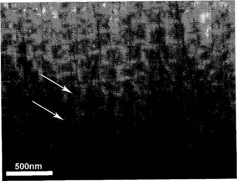
However, due to the large lattice mismatch between AlN and sapphire substrate and the high dislocation density (~10 10 cm -2 ), so how to obtain AlN films with low dislocation density is still a difficult problem

Method used


Image

  • AIN film preparing method
  • AIN film preparing method
  • AIN film preparing method

Examples


preparation example Construction

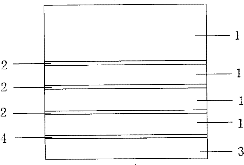
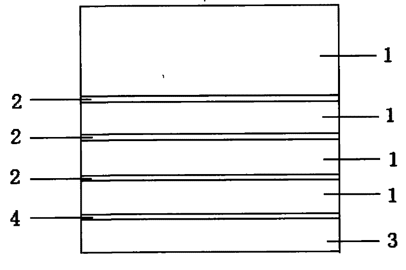
[0018] A method for preparing an AlN thin film, characterized in that:

[0019] 1.1 In the epitaxial film growth chamber, Al 2 0 3 , SiC or Si is the substrate 3, and the substrate 3 is nitrided at a temperature of 800-850° C. for 10-30 minutes;

[0020] 1.2. A 10-20nm AlN (aluminum nitride) buffer layer 4 is grown at 500-765°C;

[0021] 1.3. Growing the AlN epitaxial layer 1 in an environment greater than 780°C;

[0022] 1.4. In the process of growing the AlN epitaxial layer 1, every time the AlN epitaxial layer 1 grows 100-500 nm, a layer of 10-20 nm AlN insertion layer 2 is grown at 500-765 ° C, and the growth interruption method is used to interrupt the AlN grow for 0.5-3 minutes, and then continue to grow the AlN epitaxial layer 1 in an environment greater than 780° C., repeating this cycle until the required number of layers is obtained.

[0023] Moreover, the number of AlN insertion layers 2 is 3 to 8 layers.

[0024] Moreover, the AlN buffer layer 4 is grown by pu...

Embodiment 1

[0028] Select two inches of Al 2 o 3 As the substrate 3, the substrate 3 was cleaned at 810° C. for 10 minutes before growth. Nitriding the substrate 3 at 800°C for 10 minutes, then growing a 10nm AlN buffer layer 4 at 500°C, and then growing a 1.8μm AlN epitaxial layer 1 at 780°C; in the process of growing the AlN epitaxial layer 1 In this method, for every 100nm AlN epitaxial layer growth, a 10nm AlN insertion layer 2 was grown at 500°C, and the AlN growth was interrupted for 0.5 minutes, and then the AlN epitaxial layer 1 was continued to grow at 800°C.

Embodiment 2

[0030] Two inches of Si was selected as the substrate 3, and the substrate 3 was cleaned at 810°C for 10 minutes before growth. Nitriding the substrate 3 at 850°C for 30 minutes, then growing a 20nm AlN buffer layer 4 at 765°C, and then growing a 1.8μm AlN epitaxial layer 1 at 800°C; during the process of growing the AlN epitaxial layer 1 , every time a 500nm AlN epitaxial layer is grown, a 20nm AlN insertion layer 2 is grown at 765°C, and the AlN growth is interrupted for 3 minutes, and then the AlN epitaxial layer 1 is grown at 800°C, and the number of AlN insertion layers 2 is 8 floors.


PUM


Abstract

The invention discloses a preparation method of AlN membranes, which is characterized in that: 1.1 Al2O3, SiC or Si are taken as an underlayer which is subjected to nitridation for 10min to 30min in an extending membrane growth chamber at the temperature of 800 DEG C to 850 DEG C; 1.2 an AIN buffer layer of 10nm to 20nm grows at the temperature of 500 DEG C to 765 DEG C; 1.3 an extending layer ofAIN grows at the temperature over 780 DEG C; 1.4 during the growth of the extending layer of AIN, an AIN inserting layer of 10nm to 20nm grows at the temperature of 500 DEG C to 765 DEG C, following the growth of each 100nm to 500nm of the extending layer of AIN, a growth interruption to the AIN for 0.5min to 3min is carried out by using growth interruption method, and then the extending layer ofAIN continues to grow at the temperature over 780 DEG C; and the processes of growth and interruption are repeated till obtain the required layers. The preparation method has the advantages that the AIN membrane with mirror-like and smooth surface but without cracks can be obtained, the performance parameters, such as the not more than 255-arcsec of full width at half maximum of a rocking curve of X-ray diffraction (002) surface with high resolution, the not more than 290-arcsec of full width at half maximum of a rocking curve of (105) surface, the lower than 5 multiplied by 10<8> cm <-2> of edge dislocation density and the not more than 0.29nm in the range of 4Mum multiplied by 4Mum of the smoothness of the surface, can be obtained.

Description

technical field [0001] The invention relates to a method for preparing a film, in particular to a method for preparing an AlN thin film. Background technique [0002] With the continuous in-depth research on the first-generation silicon semiconductor materials and the second-generation gallium arsenide semiconductor materials, the application of their devices is becoming more and more limited. Modern technology also needs materials with high temperature resistance, high frequency, high power, good chemical stability and work in strong radiation environment in more fields. eV) has received great attention, and these materials include AlN, SiC, GaN and so on. Among them, AlN is the representative of the third-generation direct wide bandgap semiconductor material, which has the characteristics of wide bandgap, high critical breakdown electric field, high thermal conductivity, high carrier saturation drift velocity and high chemical stability. In particular, AlN has similar th...

Claims


Application Information

Patent Timeline
Patent Type & Authority Patents(China)
IPC IPC(8): H01L21/20H01L21/205
Inventor 刘昌付秋明刘博
Owner 常熟紫金知识产权服务有限公司
Learn More