
Static random access memory unit

A static random access, memory cell technology, applied in static memory, digital memory information, information storage, etc., can solve problems such as failure to be widely used, threshold voltage loss, voltage difference, etc.

Active Publication Date: 2015-01-28
INST OF MICROELECTRONICS CHINESE ACAD OF SCI
View PDF4 Cites 4 Cited by
  • Summary
  • Abstract
  • Description
  • Claims
  • Application Information

AI Technical Summary

Problems solved by technology

However, due to the following disadvantages of the SRAM unit, it has not been widely used
First, there is a loss of threshold voltage in a single NMOS or PMOS
figure 2 There is a voltage difference between the drains of M1 and M3, making the storage node susceptible to noise
Secondly, due to the delay caused by the addition of transistors on the critical path, the read and write speeds are very slow

Method used


Image

  • Static random access memory unit
  • Static random access memory unit
  • Static random access memory unit

Examples


Embodiment Construction

[0023] In order to make the object, technical solution and advantages of the present invention clearer, the present invention will be described in further detail below in conjunction with specific embodiments and with reference to the accompanying drawings.

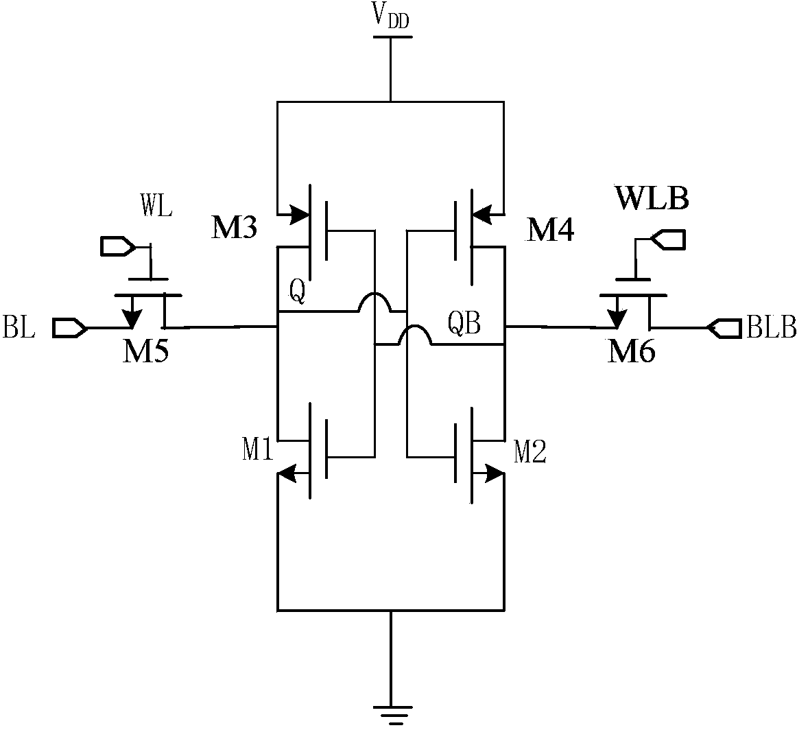
[0024] Such as image 3 as shown, image 3 It is a circuit diagram of a static random access memory unit provided by an embodiment of the present invention, including:

[0025] The first inverter includes a first NMOS transistor M1 and a first PMOS transistor M3, and has a first self-stabilizing capacitor between the first NMOS transistor M1 and the first PMOS transistor M3;

[0026] The second inverter includes a second NMOS transistor M2 and a second PMOS transistor M4, with a second self-stabilizing capacitor between the second NMOS transistor M2 and the second PMOS transistor M4; and

[0027] The first and second read-write control units are respectively connected to one end of the first self-stabilizing capacitor a...


PUM


Abstract

The invention discloses a static random access memory unit, which comprises a first inverter which includes a first N-channel metal oxide semiconductor (NMOS) transistor and a first P-channel metal oxide semiconductor (PMOS) transistor, wherein a first self-stabilizing capacitor is arranged between the first NMOS transistor and the first PMOS transistor, a second inverter which includes a second NMOS transistor and a second PMOS transistor, wherein a second self-stabilizing capacitor is arranged between the second NMOS transistor and the second PMOS transistor, and a first reading and writing control unit and a second reading and writing control unit which are connected to one end of the first self-stabilizing capacitor and one end of the second self-stabilizing capacitor respectively, wherein the first self-stabilizing capacitor and the second self-stabilizing capacitor, together with one end of the first reading and writing control unit and one end of the second reading and writing control unit, are connected to different MOS transistors respectively. The static random access memory unit disclosed by the invention can effectively resist radiated interference, effectively reduce circuit area and save manufacturing cost.

Description

technical field [0001] The present invention relates to the technical field of static random access memory (SRAM), and more particularly, to a static random access memory unit. Background technique [0002] According to the data storage method, semiconductor memory is divided into dynamic random access memory (DRAM), non-volatile memory and static random access memory (SRAM). SRAM has established its unique advantage by being able to achieve fast operating speeds in a simple and low power consumption manner. Also, compared to DRAM, SRAM is relatively easy to design and manufacture because it does not need to periodically refresh the stored information. [0003] Generally, an SRAM cell consists of two drive transistors, two load devices, and two access transistors. According to the type of load devices contained, SRAM itself can be divided into complete complementary metal-oxide-semiconductor (CMOS) SRAM, high load resistance (High Load Resistor) SRAM and thin film transist...

Claims


Application Information

Patent Timeline
IPC IPC(8): G11C11/413
Inventor 刘梦新刘鑫赵发展韩郑生
Owner INST OF MICROELECTRONICS CHINESE ACAD OF SCI
Learn More